Carbene metal complexes as OLED materials
a carbene metal complex and metalcarbene technology, applied in the field of organic light emitting devices, can solve the problems of not being sufficiently stable for commercial devices and well known applications of carbene ligands in photochemistry, and achieve the effect of high-energy phosphorescent emitters
- Summary
- Abstract
- Description
- Claims
- Application Information
AI Technical Summary
Benefits of technology
Problems solved by technology
Method used
Image
Examples
example 1
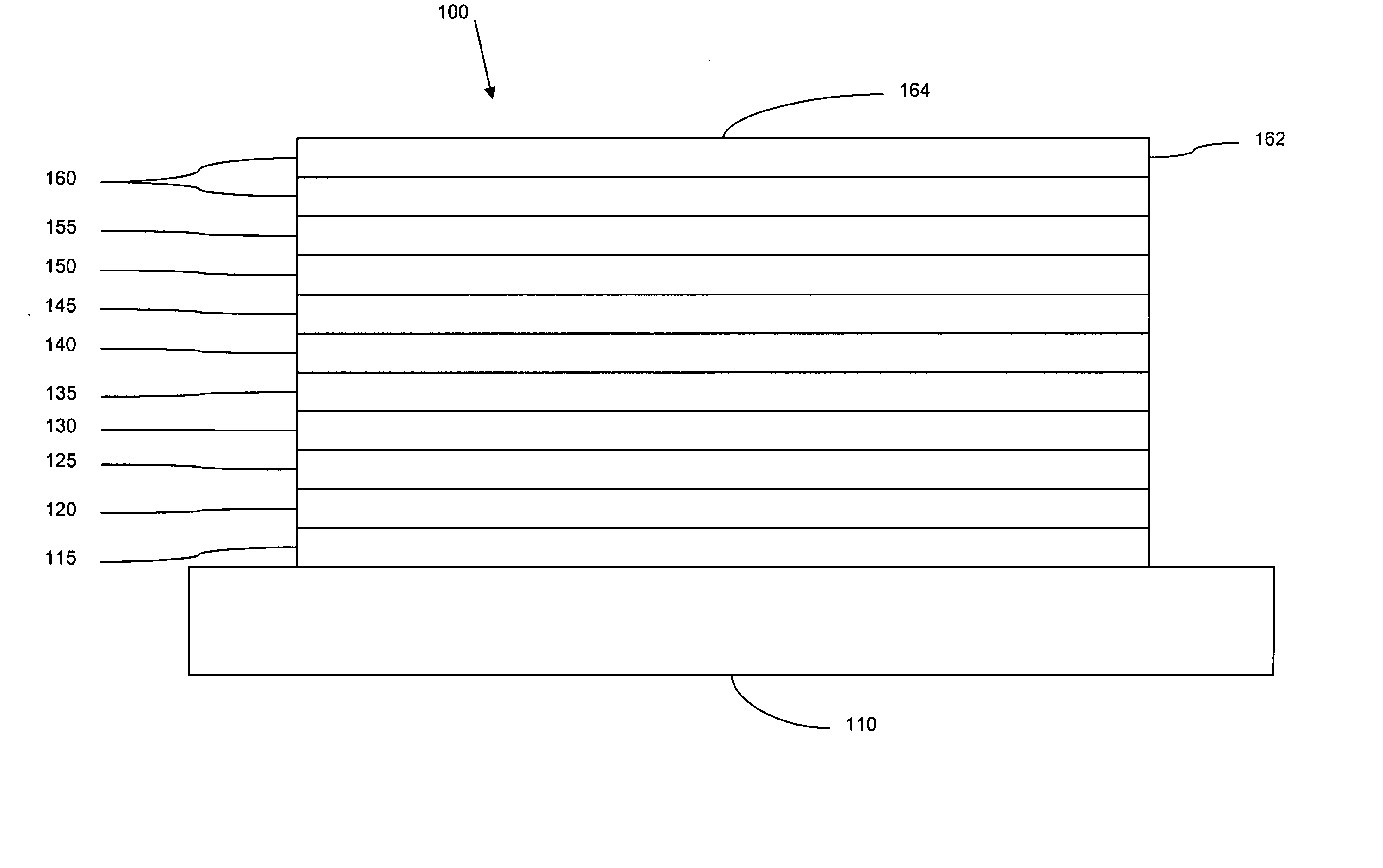
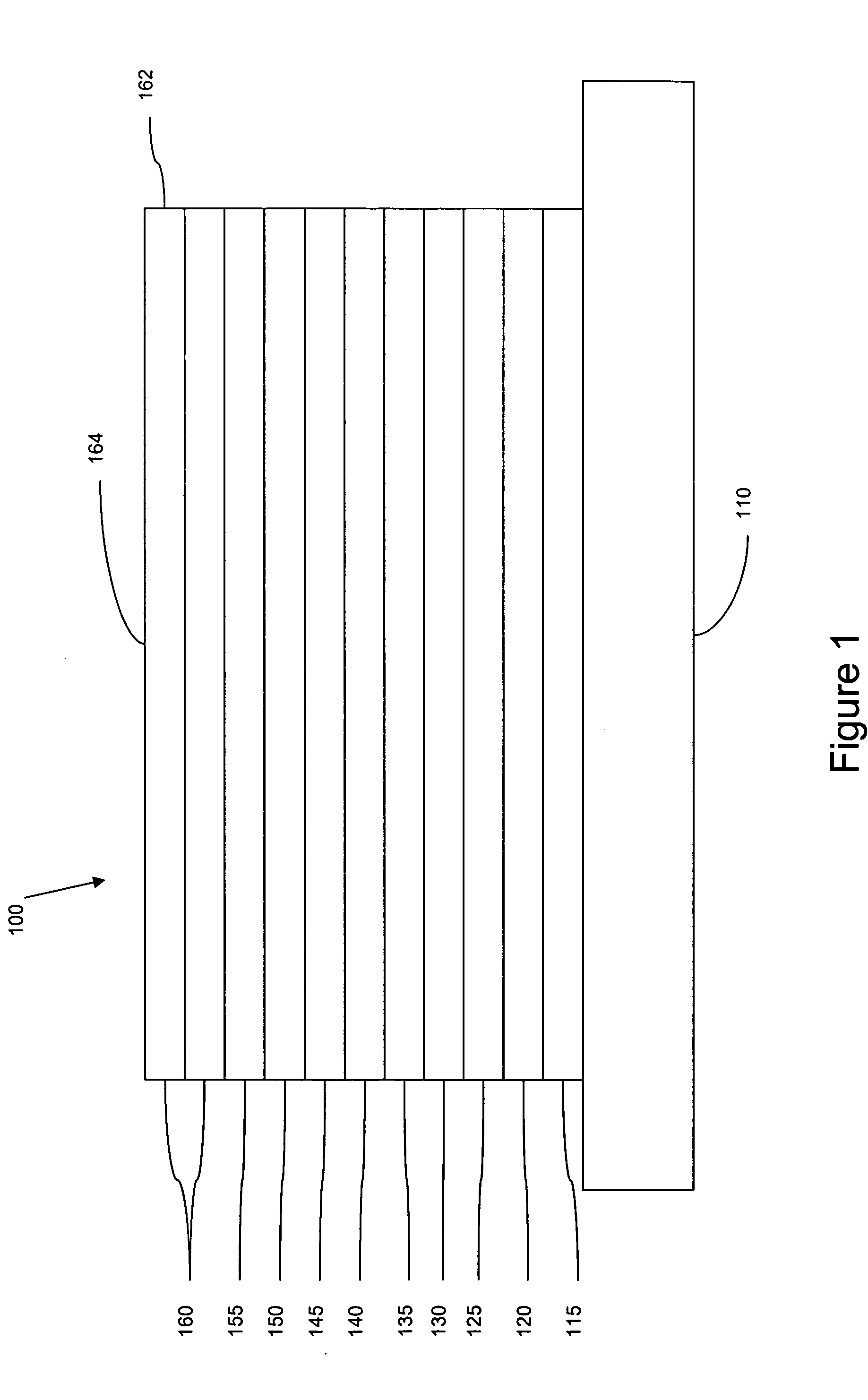
[0091] The organic stack consisted of sequentially, from the ITO surface, 100 Å thick of copper phthalocyanine (CuPc) as the hole injection layer (HIL), 300 Å of 4,4′-bis[N-(1-naphthyl)-N-phenylamino]biphenyl (α-NPD), as the hole transporting layer (HTL), 300 Å of 1,3-N,N-dicarbazole-benzene (mCP) doped with 6 wt % dopant A as the emissive layer (EML), 400 Å of aluminum(III)bis(2-methyl-8-hydroxyquinolinato)4-phenylphenolate (BA1q) as the ETL2. There was no ETL1.
example 2
[0092] The organic stack consisted of sequentially, from the ITO surface, 100 Å thick of copper phthalocyanine (CuPc) as the hole injection layer (HIL), 300 Å of 4,4′-bis[N-(1-naphthyl)-N-phenylamino]biphenyl (α-NPD), as the hole transporting layer (HTL), 300 Å of 1,3-N,N-dicarbazole-benzene (mCP) doped with 6 wt % of dopant A as the emissive layer (EML), and 100 Å of 2,3,6,7,10,11-hexaphenyltriphenylene (HPT) as the ETL2, and 400 Å of aluminum(III)bis(2-methyl-8-hydroxyquinolinato)4-phenylphenolate (BA1q) as the ETL1. FIG. 3 shows plots of current vs. voltage of device CuPc(100 Å) / NPD(300 Å) / mCP:dopant A(300 Å,6%) / BA1Q(400 Å) and device CuPc(100 Å) / NPD(300 Å) / mCP:dopant A(300 Å,6%) / HPT(100 Å) / BA1Q(400 Å).
[0093]FIG. 4 shows plots of quantum efficiency vs. current density for device CuPc(100 Å) / NPD(300 Å) / mCP: dopant A(300 Å,6%) / BA1Q(400 Å) and device CuPc(100 Å) / NPD(300 Å) / mCP:dopant A(300 Å,6%) / HPT(100 Å) / BA1Q(400 Å).
[0094]FIG. 5 shows the electroluminescent spectra for device Cu...
example 3
[0096] The organic stack consisted of sequentially, from the ITO surface, 100 Å thick of copper phthalocyanine (CuPc) as the hole injection layer (HIL), 300 Å of 4,4′-bis[N-(1-naphthyl)-N-phenylamino]biphenyl (α-NPD), as the hole transporting layer (HTL), 300 Å of 1,3-bis(triphenylsilyl)benzene (UGH5) doped with 12 wt % dopant A as the emissive layer (EML), 400 Å of aluminum(III)bis(2-methyl-8-hydroxyquinolinato)4-phenylphenolate (BA1q) as the ETL2. There was no ETL1.
PUM
| Property | Measurement | Unit |
|---|---|---|
| Energy | aaaaa | aaaaa |
| Structure | aaaaa | aaaaa |
Abstract
Description
Claims
Application Information


