Lighting device

a technology of light source and transparent electrode, which is applied in outdoor lighting, planar light sources, lighting and heating apparatus, etc., can solve the problems of low luminance, voltage drop, and high resistivity of transparent conductive film, and achieve favorable in-plane luminance uniformity

Active Publication Date: 2005-11-24
SEMICON ENERGY LAB CO LTD
View PDF14 Cites 76 Cited by
  • Summary
  • Abstract
  • Description
  • Claims
  • Application Information

AI Technical Summary

Benefits of technology

[0020] According to the invention, a lighting device having favorable in-plane uniformity of luminance can be obtained. Since an auxiliary electrode is not placed in the direction of light emission, little light is lost due to the auxiliary electrode, and a material, a thickness, or a formation position of the auxiliary electrode can be freely set.

Problems solved by technology

However, a transparent conductive film which is typically used as a transparent electrode often has relatively high resistivity, and voltage drop is caused in a portion away from a current supply terminal.
Therefore, voltage drop is caused in a portion away from a current supply terminal, which results in low luminance.
However, the auxiliary electrode can only be partly provided, because light emitted from a light emitting layer cannot be extracted outside when the auxiliary electrode is entirely provided on the anode in the structure of Reference 1.

Method used


Image

  • Lighting device
  • Lighting device
  • Lighting device

Examples


embodiment mode 1

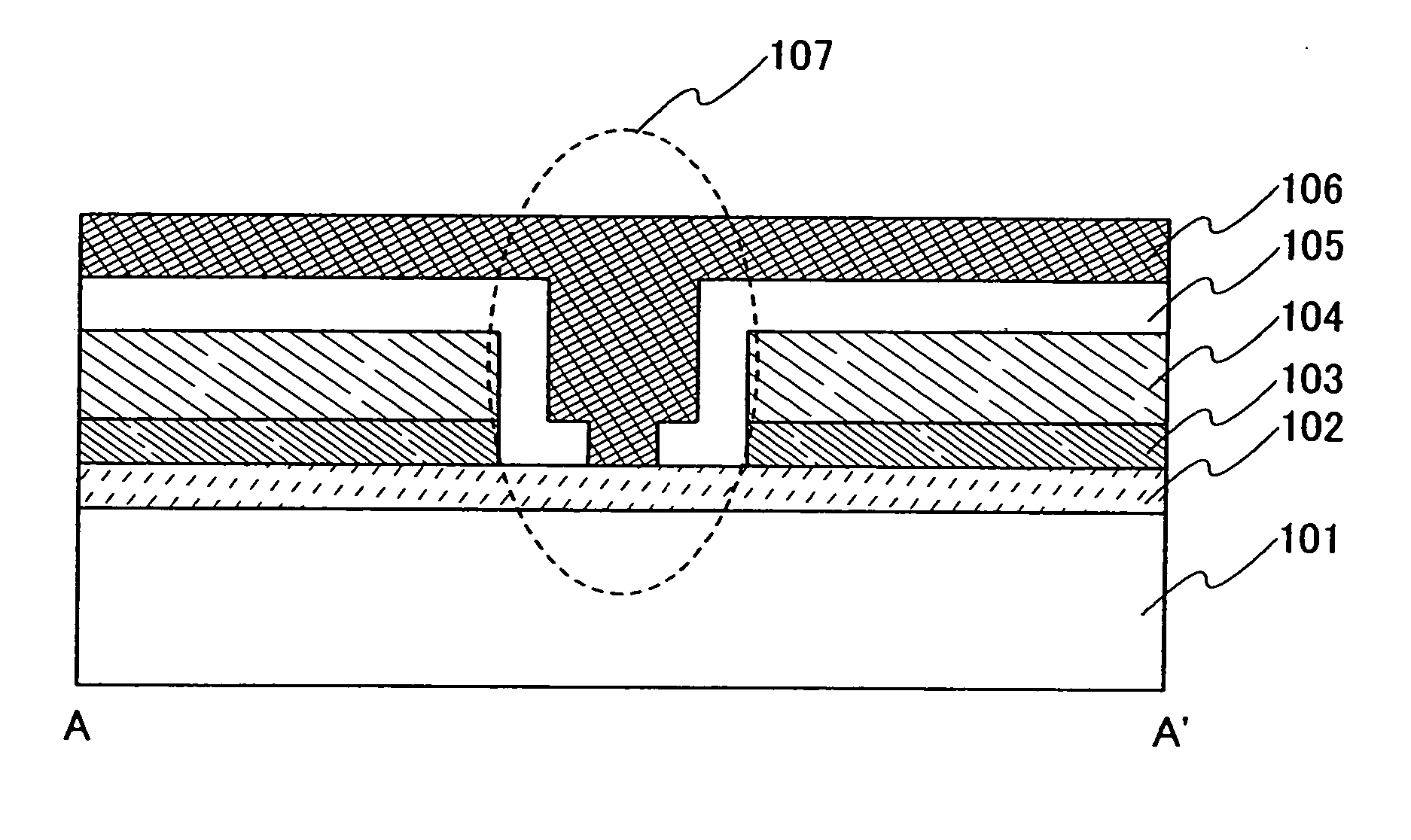
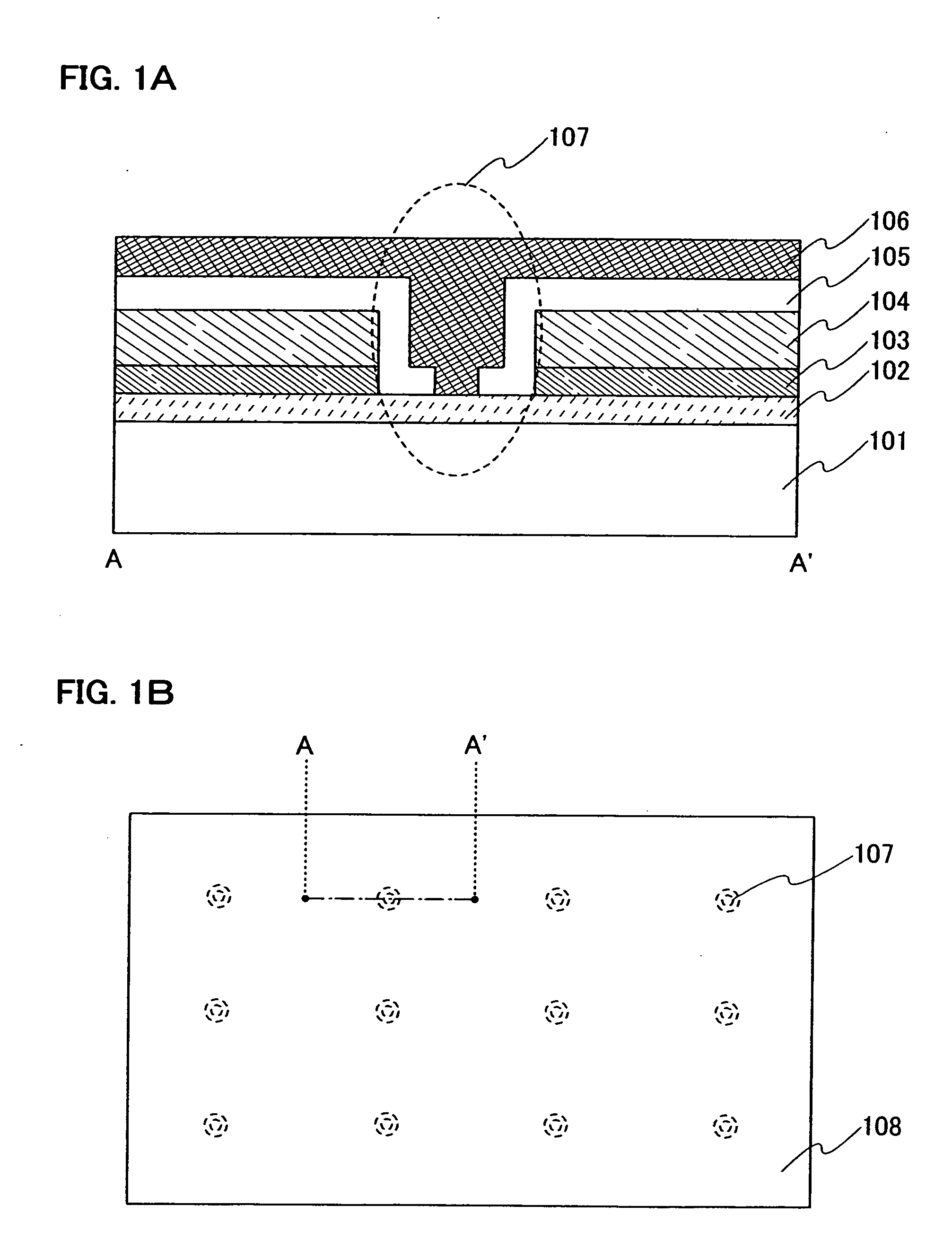
[0034] A structure of a lighting device of the invention is described with reference to FIGS. 1A and 1B. A lighting device shown in FIGS. 1A and 1B is a bottom emission lighting device which emits light from a substrate side. Note that FIG. 1B is a top view of a light emitting region in a lighting device of the invention and FIG. 1A is a cross-sectional view (taken along line A-A′ in FIG. 1B) of the vicinity of an opening in the light emitting region.

[0035] In FIGS. 1A and 1B, a light transmitting substrate is used as a substrate 101. Specifically, a light transmitting material such as glass, plastic, polyester resin, or acrylic resin can be used. The substrate 101 may be flexible.

[0036] A transparent conductive film is formed over the substrate 101 as a first electrode 102. For example, indium tin oxide (hereinafter referred to as ITO), indium tin oxide containing silicon, indium oxide containing zinc oxide (ZnO) of 2% to 20%, or the like can be used for the transparent conductiv...

embodiment mode 2

[0054] A structure of a lighting device of the invention is described with reference to FIGS. 5A and 5B. A lighting device shown in FIGS. 5A and 5B is a top emission lighting device which emits light from the opposite side of a substrate side. Note that FIG. 5B is a top view of a light emitting region of a lighting device and FIG. 5A is a cross-sectional view (taken along line A-A′ in FIG. 5B) of the vicinity of an opening in the light emitting region.

[0055] In FIGS. 5A and 5B, a thin substrate formed of a flexible material is used as a substrate 501. Specifically, a flexible substrate such as a plastic substrate, more specifically a polyester film or an acrylic resin film, can be used.

[0056] A second electrode 502 is formed over the substrate 501. A known material can be used for the second electrode 502. In the case of using the second electrode 502 as a cathode, a conductive material having a low work function is preferably used. Rare earth metal such as Yb or Er can be used to...

embodiment 1

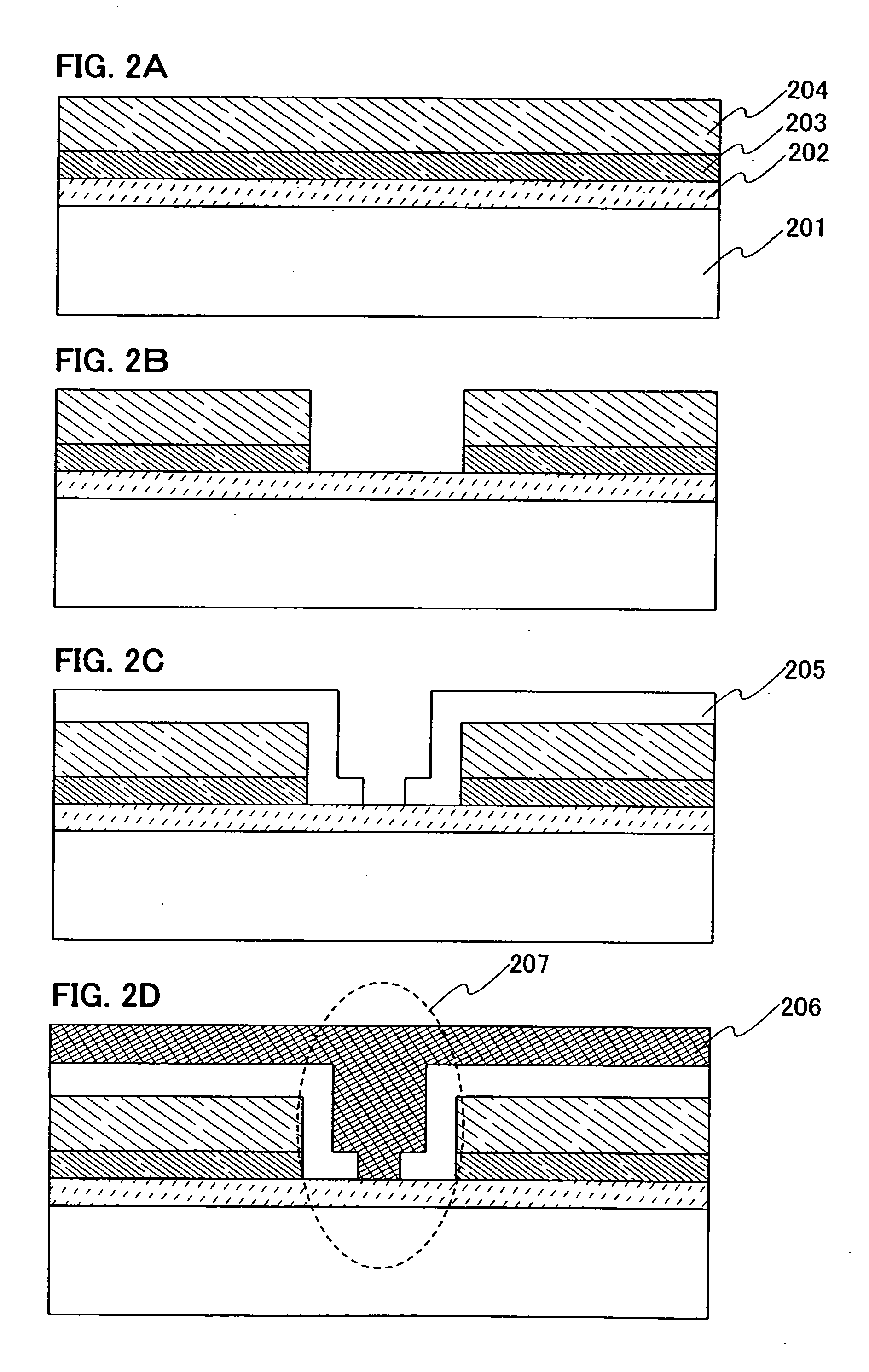
[0064] A method for manufacturing the lighting device of the invention shown in FIGS. 1A and 1B is described in this embodiment with reference to FIGS. 2A to 2D.

[0065] A transparent conductive film serving as a first electrode 202 is formed over a light transmitting substrate 201. In this embodiment, a glass substrate is used as the light transmitting substrate 201 and an ITO film is formed for forming the first electrode 202.

[0066] A layer including a light emitting material 203 is formed over the first electrode 202. A known material can be used for the layer including a light emitting material 203. The layer including a light emitting material may have a laminated structure of a plurality of layers each including a light emitting material.

[0067] A second electrode 204 is formed over the layer including a light emitting material 203 (FIG. 2A). The second electrode 204 has an opening. After the second electrode is entirely formed over the layer including a light emitting materia...


PUM


Abstract

An object of the invention is to provide a lighting device which can suppress luminance nonuniformity in a light emitting region when the lighting device has large area. A layer including a light emitting material is formed between a first electrode and a second electrode, and a third electrode is formed to connect to the first electrode through an opening formed in the second electrode and the layer including a light emitting material. An effect of voltage drop due to relatively high resistivity of the first electrode can be reduced by electrically connecting the third electrode to the first electrode through the opening.

Description

BACKGROUND OF THE INVENTION [0001] 1. Field of the Invention [0002] The present invention relates to a lighting device using a light emitting element. [0003] 2. Description of the Related Art [0004] A light emitting element is a self light emitting element and is attempted to be used as a lighting device. The light emitting element is a surface-emitting body, and a lighting device capable of emitting near-natural light can be obtained by using the light emitting element for lighting. [0005] The light emitting element has an anode, a cathode, and a layer including a light emitting material which provides luminescence (Electroluminescence) by applying an electric field thereto. A hole injected from the anode is combined with an electron injected from the cathode in the layer including a light emitting material, thereby obtaining luminescence. Luminescence obtained from the layer including a light emitting material includes luminescence (fluorescence) that is obtained in returning from...

Claims


Application Information

Patent Timeline
Patent Type & Authority Applications(United States)
IPC IPC(8): H05B33/26H01L27/15H01L51/50H01L51/52H05B33/14H05B33/28
CPCH01L33/382H01L51/5203H01L51/5212H01L2251/5361H01L2251/5338F21W2131/101F21Y2105/00H10K50/814H10K2102/311H10K59/805H10K50/805
Inventor ARAI, YASUYUKI
Owner SEMICON ENERGY LAB CO LTD
Why Eureka
Try Eureka