Plasma display device

a technology of display device and plasma, which is applied in the direction of identification means, electrical apparatus casings/cabinets/drawers, instruments, etc., can solve the problems of large heat generation, large screen, and large weight of the display device, and achieve the effect of increasing the heat dissipation area of the heat transferred from the integrated circuit module 15

Inactive Publication Date: 2005-11-24
SAMSUNG SDI CO LTD
View PDF10 Cites 44 Cited by
  • Summary
  • Abstract
  • Description
  • Claims
  • Application Information

AI Technical Summary

Benefits of technology

[0044] The integrated circuit module 15, in which the heat is dissipated through the heat sink 19, is provided at many positions on a circuit board assembly 13. In order to enhance the advantage of the invention, the integrated circuit module 15 is in an exemplary embodiment provided at the edge of the circuit board assembly 13. Further, the heat sink 19 may be provided separately for each integrated circuit module 15 or may be provided commonly to adjacent integrated circuit modules 15. Further, in the design of the circuit board assembly 13, the integrated circuit module 15 may be arranged at the edge of the circuit board assembly 13.
[0045] The heat sink 19 of the present embodiment may be applied to all integrated circuit modules 15 provided on the circuit board assembly 13 or may be selectively applied to only the integrated circuit modules 15 which are provided at the edge of the circuit board assembly 13.
[0046] As shown in FIG. 3, the heat sink 19 of the present embodiment has a U-shape section, including a first, second, and third portions 19a, 19b, and 19c. The heat sink 19 is provided on the integrated circuit module 15 which is disposed at the edge of the circuit board assembly 13. The first portion 19a is attached to the integrated circuit module 15 and the second portion 19b is bent toward the chassis base 5 from the first portion 19a. Further, the third portion 19c is formed integrally with the second portion 19b and is bent horizontally to the first portion 19a to be attached to the chassis base 5.
[0047] More specifically, an inner surface of the first portion 19a of the heat sink 19 is attached to a top surface of the integrated circuit module 15 and an outer surface of the third portion 19c is attached to the chassis base 5. The second portion 19b connects the first portion 19a to the third portion 19c, thereby forming the heat conduction structure.
[0048] The first portion 19a is attached to the integrated circuit module 15 so as to make substantial contact with the entire top surface of the integrated circuit module. The third portion 19c is attached to the chassis base 5 so as to make substantial contact with the surface of the chassis base 5.
[0049] As such, the heat sink 19 having the first, second, third portions 19a, 19b, 19c, respectively, can be implemented in various shapes. When the integrated circuit module 15 is disposed at the edge of the circuit board assembly 13, the heat sink 19 may be in a U-shape section. With the heat sink 19, the heat dissipating area of the heat transferred from the integrated circuit module 15 is increased.

Problems solved by technology

Further, it may be lightweight, thin, and have a large screen.
However, large currents which flow in the respective integrated circuit modules provided on the circuit board assemblies result in a significant amount of heat being generated.
If the heat is not sufficiently dissipated to the outside, the integrated circuit modules may cease to operate properly.
However, the noise generated from the fan inconveniences the user.
However, this structure has a limit to the amount of heat dissipation of the integrated circuit module and the entire circuit board assembly.

Method used


Image

  • Plasma display device
  • Plasma display device
  • Plasma display device

Examples


Embodiment Construction

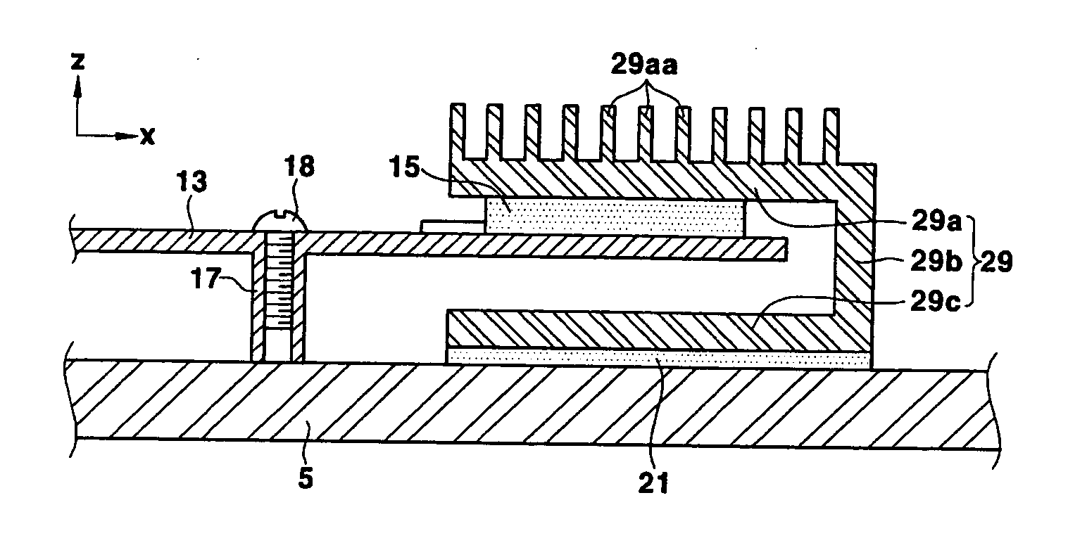
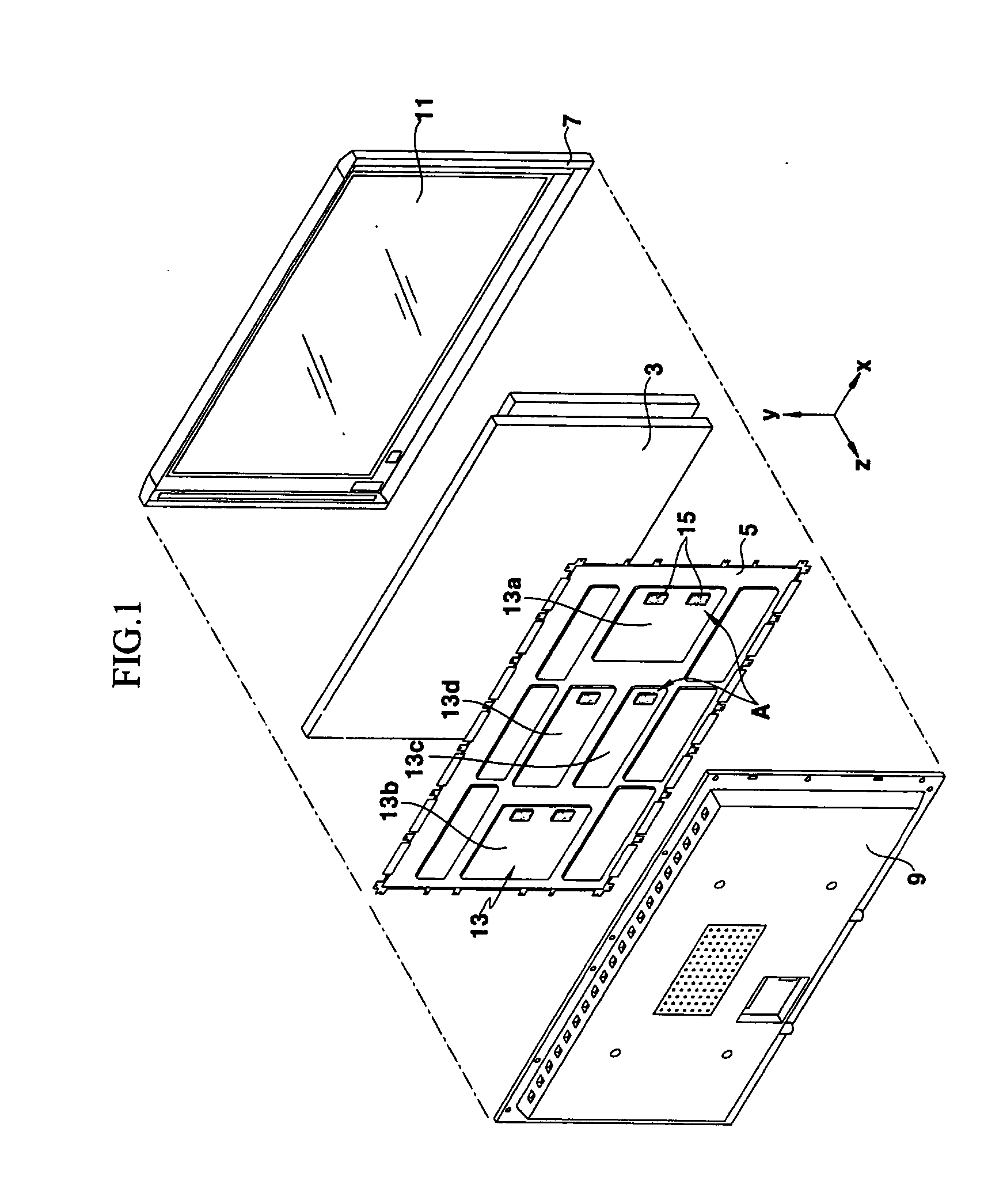
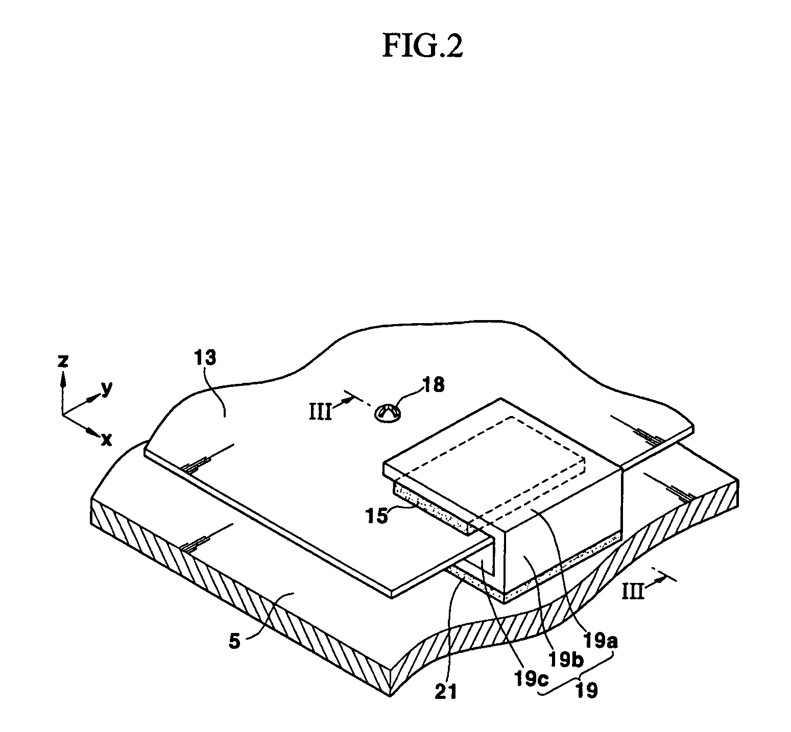
[0035] Referring to FIG. 1, an exemplary embodiment of a plasma display device of the present invention has a PDP 3 that displays images and a chassis base 5 that is coupled to a surface of the PDP 3 that is opposite to a display surface of the PDP 3. Further, the plasma display device has a front cover 7 that is disposed over the PDP 3 and a back cover 9 that is disposed over the chassis base 5.

[0036] A heat dissipating sheet (not shown) may be arranged between the PDP 3 and the chassis base 5 to transfer heat generated in the PDP 3 to the chassis base 5. Further, a filter 11 may be mounted on the front cover 7 so as to shield electromagnetic waves emitted from the PDP 3.

[0037] Typically, the PDP 3 has a substantially quadrangular shape (in FIG. 1, a rectangular shape in which the length in the X direction is longer than the length in the Y direction). The chassis base 5 has a shape similar to the PDP 3 and is made of a material, such as aluminum, having superior heat conductivit...


PUM


Abstract

A plasma display device that diversifies heat dissipating paths of integrated circuit modules in a circuit board assembly, thereby enhancing heat dissipation of the integrated circuit modules. The plasma display device includes a plasma display panel, a chassis base on which the plasma display panel is attached and supported, integrated circuit modules that are mounted on the circuit board assembly on an opposite side of the chassis base to the plasma display panel, and heat sinks, each being attached to one side of each of the integrated circuit modules to dissipate heat therefrom. The heat sink is formed such that one end thereof extends to come in contact with the chassis base.

Description

CROSS-REFERENCES TO RELATED APPLICATION [0001] This application claims priority to and the benefit of Korean Patent Application No. 10-2004-0035144 filed on May 18, 2004 and Korean Patent Application No. 10-2005-0031870 filed on Apr. 18, 2005, in the Korean Intellectual Property Office, the entire disclosures of which are incorporated herein by reference. BACKGROUND OF THE INVENTION [0002] 1. Technical Field [0003] The present invention relates to a plasma display device and, more particularly, to a plasma display device that can efficiently dissipate heat from switching elements or integrated circuit modules arranged on circuit board assemblies. [0004] 2. Description of the Related Art [0005] Generally, a plasma display panel (hereinafter referred to as a PDP) is a display panel in which vacuum ultraviolet rays generated by gas discharge in discharge cells excite phosphors to produce images. The PDP has display configurations, including superior display capacity, brightness, contra...

Claims


Application Information

Patent Timeline
Patent Type & Authority Applications(United States)
IPC IPC(8): G09F9/00H01L23/36H01J17/28H05K5/00H05K7/20
CPCH05K7/20963H01L2924/0002H01L2924/00
Inventor HAN, CHAN-YOUNGHA, SEUNG-IIJEON, YOUNG-JUN
Owner SAMSUNG SDI CO LTD
Why Eureka
Try Eureka