
Method for manufacturing carbon nanotube field emission display

a carbon nanotube and field emission technology, applied in the manufacture of electrode assemblies, electric discharge tubes/lamps, electrode systems, etc., can solve the problems of reducing so as to improve the efficiency of electron emission and improve the effect of electron emission efficiency and high resolution

Active Publication Date: 2005-12-01
TSINGHUA UNIV +1
View PDF0 Cites 27 Cited by
  • Summary
  • Abstract
  • Description
  • Claims
  • Application Information

AI Technical Summary

Benefits of technology

The present invention provides a method for manufacturing a carbon nanotube field emission display with high resolution and good display quality. The method includes the steps of dispersing carbon nanotubes on cathode electrodes, forming insulation beams and gate electrodes, making the carbon nanotubes stand vertically on the cathode electrodes, and packing and sealing a phosphor screen and side walls. Compared with conventional field emission displays, the carbon nanotube field emission display has the advantage of having carbon nanotubes surround the gate electrodes and act as electron emitters, which ensures the gate electrodes have the dual functions of driving electrons and focusing emitted electrons.

Problems solved by technology

Diode type structures are unsuitable for applications requiring high resolution displays, because the diode type structures require high voltages, produce relatively non-uniform electron emissions, and require relatively costly driving circuits.
The greater the value of L / S, the more electrons are lost, and the lower the efficiency of electron emission.

Method used


Image

  • Method for manufacturing carbon nanotube field emission display
  • Method for manufacturing carbon nanotube field emission display
  • Method for manufacturing carbon nanotube field emission display

Examples


Embodiment Construction

[0031] Reference will now be made to the drawings to describe a preferred embodiment of the present invention in detail.

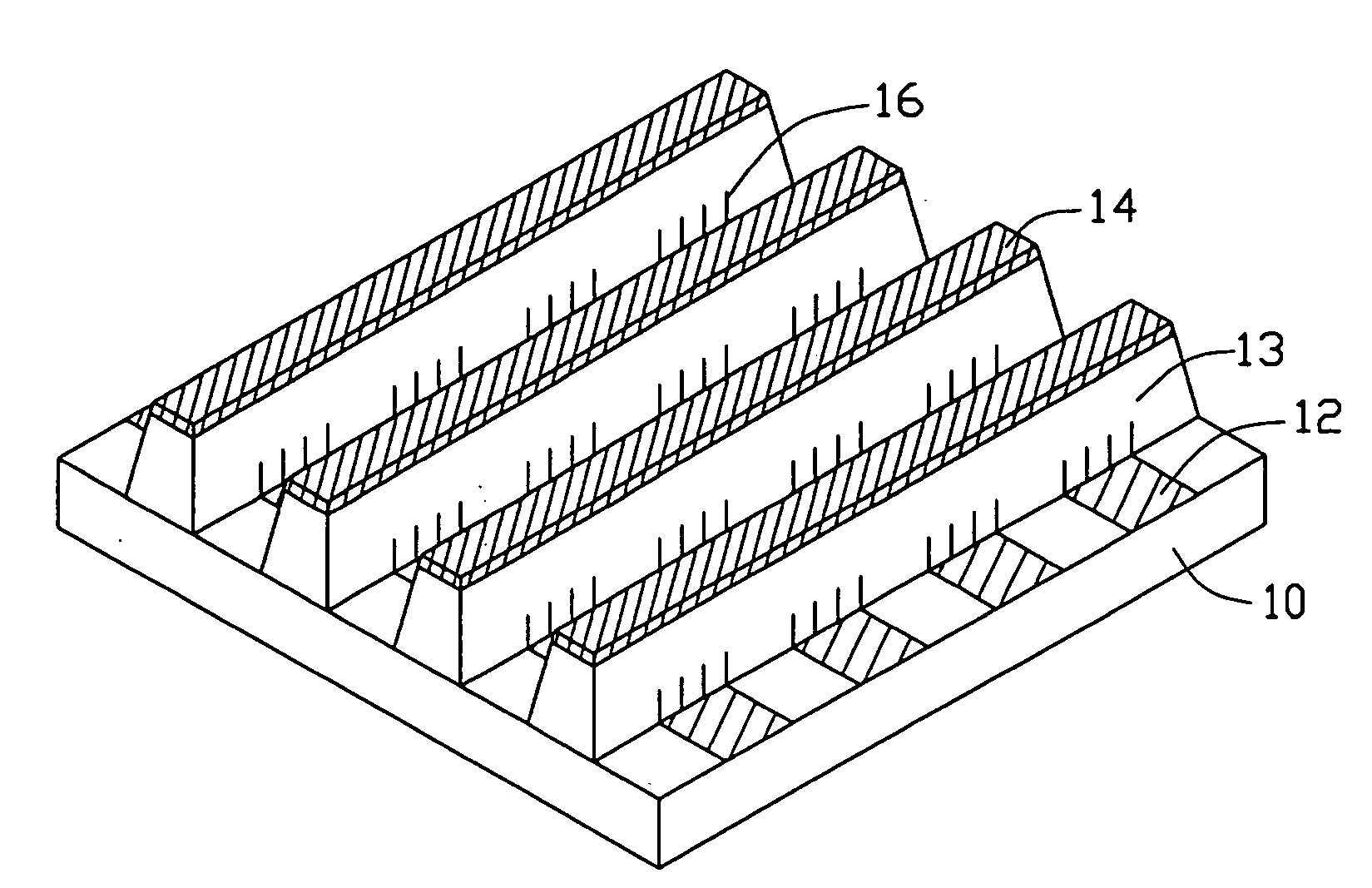
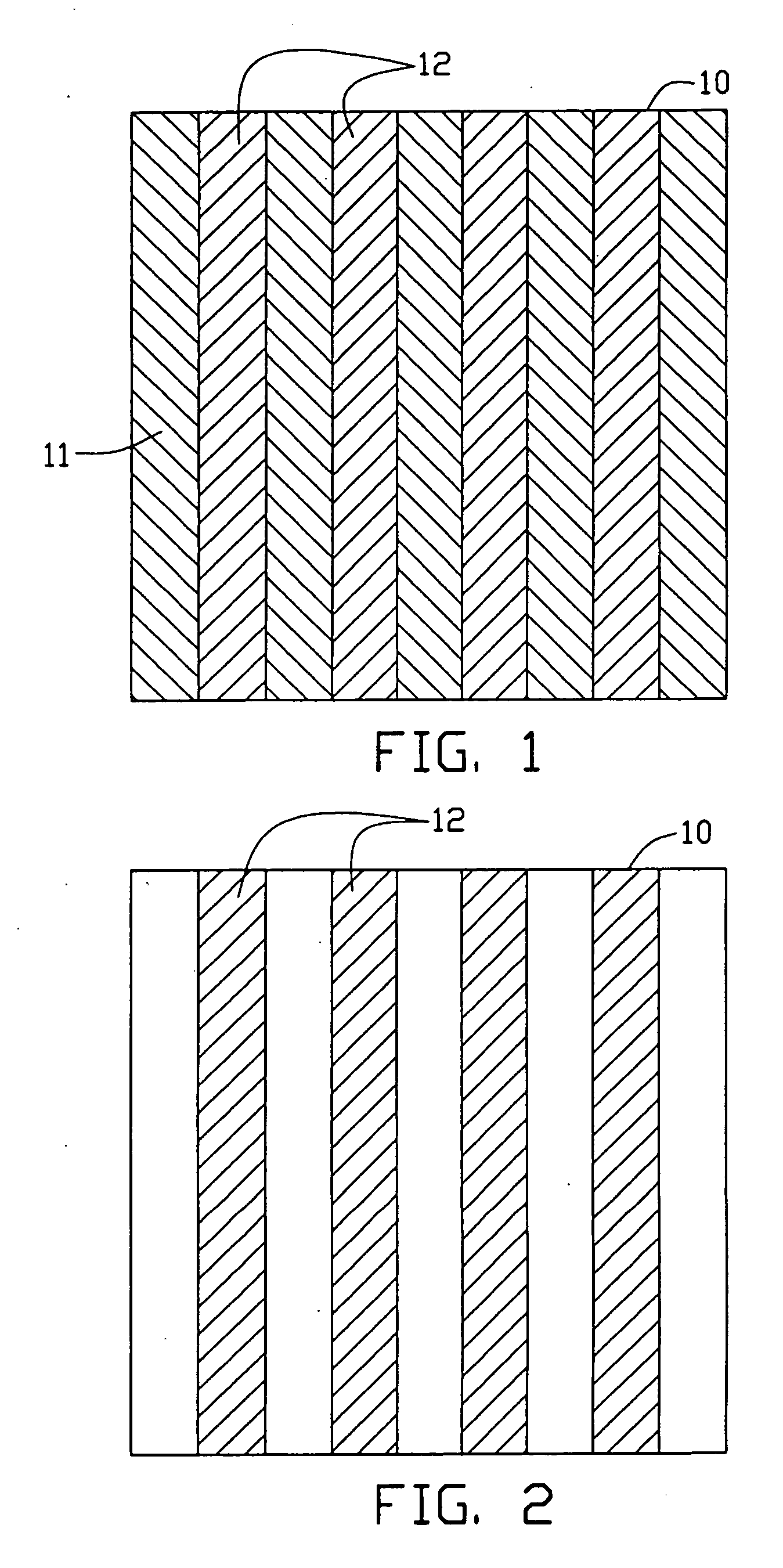
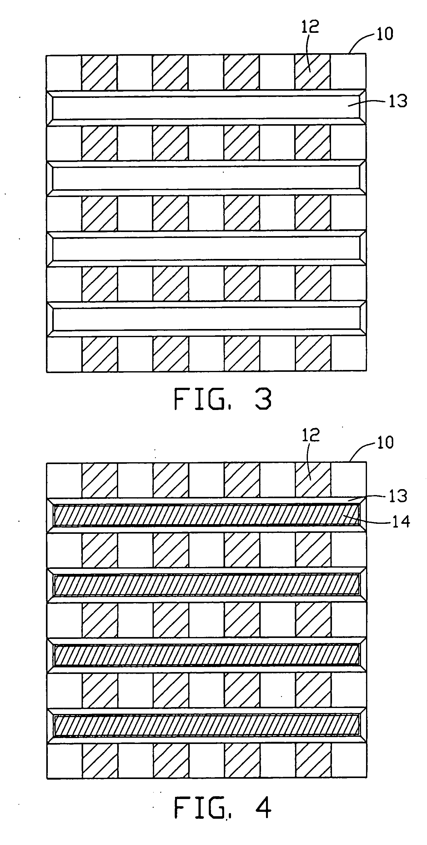
[0032] Referring initially to FIG. 6, a carbon nanotube field emission display 1 manufactured by a method in accordance with a preferred embodiment of the present invention is shown. The field emission display 1 includes: an array of parallel cathode electrodes 12 formed on an insulative substrate 10; an array of parallel insulation beams 13 disposed on the array of cathode electrodes 12 and being perpendicular to a lengthways direction of the cathode electrodes 12; a plurality of gate electrodes 14 made of a metallic material (preferably metal with excellent electrical conductivity) formed on tops of the insulation beams 13; a plurality of carbon nanotubes 16 functioning as electron emitters for emitting electrons, formed on portions of the cathode electrodes 12 near opposite sides of each gate electrode 14 respectively; an anode electrode 18 made of an ITO thin ...


PUM

PropertyMeasurementUnit
thickaaaaaaaaaa
thickaaaaaaaaaa
voltageaaaaaaaaaa

Abstract

A method for manufacturing a carbon nanotube field emission display includes the steps of: (a) dispersing a plurality of carbon nanotubes on an array of cathode electrodes formed on an insulative substrate; (b) forming an array of insulation beams on the array of cathode electrodes, the insulation beams being perpendicular to a lengthways direction of the cathode electrodes; (c) forming a plurality of gate electrodes on tops of the insulation beams; (d) making the carbon nanotubes located near opposite sides of each gate electrode stand vertically on the cathode electrodes; and (e) packing and sealing a phosphor screen and side walls. The gate electrodes have the dual functions of driving electron emission and focusing emitted electrons. Thereby the carbon nanotube field emission display has high resolution and good display quality.

Description

CROSS-REFERENCE TO RELATED APPLICATION [0001] This application is related to one corresponding U.S. patent applications entitled “TRIODE TYPE FIELD EMISSION DISPLAY WITH HIGH RESOLUTION,” recently filed and having the same assignee as the instant application, and having Attorney Docket No. 14963-48708. The disclosure of the above-identified application is incorporated herein by reference.BACKGROUND OF THE INVENTION [0002] The present invention relates to methods for manufacturing field emission displays, and more particularly to methods for manufacturing carbon nanotube field emission displays. [0003] Field emission displays (FEDs) are relatively new, rapidly developing flat panel display technologies. Compared to conventional technologies, e.g., cathode-ray tube (CRT) and liquid crystal display (LCD) technologies, field emission displays are superior in having a wider viewing angle, lower energy consumption, a smaller size, and a higher quality display. [0004] Generally, field emis...

Claims


Application Information

Patent Timeline
Patent Type & Authority Applications(United States)
IPC IPC(8): H01J9/02H01J9/04H01J9/12H01J9/18
CPCB82Y10/00H01J9/185H01J9/025
Inventor WEI, YANGFAN, SHOU-SHAN
Owner TSINGHUA UNIV
Learn More