Method and apparatus for high speed testing of latch based random access memory

a random access memory and latch technology, applied in the direction of digital storage, instruments, measurement devices, etc., can solve the problems of increasing the die area, affecting the test results, and causing the test results to be distorted, so as to minimize the skew of the scan enable

Inactive Publication Date: 2005-12-01
AVAGO TECH WIRELESS IP SINGAPORE PTE
View PDF6 Cites 24 Cited by
  • Summary
  • Abstract
  • Description
  • Claims
  • Application Information

AI Technical Summary

Benefits of technology

[0011] Other embodiments further include a step of substantially minimizing skew of the scan enable signal relative to each one of the latch based random access memory and a step of providing a clock tree to minimize skew of the scan enable signal relative to each one of the latch based random access memory. In additional embodiments, the scan clock signal has a falling edge in the capture cycle wherein the falling edge occurs about one-half the second scan clock period from the previous rising edge, the scan clock signal has a rising edge in the capture cycle wherein the rising edge occurs about one full second scan clock period from the previous rising edge minus about two nanoseconds, insertion delay of the scan enable signal differs from that of the scan clock signal by less than 250 picoseconds at each one of the latch based random access memory, the first scan clock period corresponds to a frequency of about 20 MHZ, and the second scan clock period corresponds to a frequency of about 62 MHz, 100 MHz, or 125 MHz.

Problems solved by technology

A key issue with the use of such a large number of memory arrays is how to test the memory arrays for manufacturing defects without increasing the die area by an excessive amount.
Application-specific integrated circuits (ASICs) are susceptible to manufacturing defects that may cause the ASIC to malfunction, called faults.
Stuck-at faults occur when a signal inside the ASIC that was designed to transition between two logic states (0 and 1) remains in one state due to a chip defect.
A transition delay fault occurs when a signal transitions too late for proper operation due to, for example, excessive net capacitance.

Method used


Image

  • Method and apparatus for high speed testing of latch based random access memory
  • Method and apparatus for high speed testing of latch based random access memory
  • Method and apparatus for high speed testing of latch based random access memory

Examples


Embodiment Construction

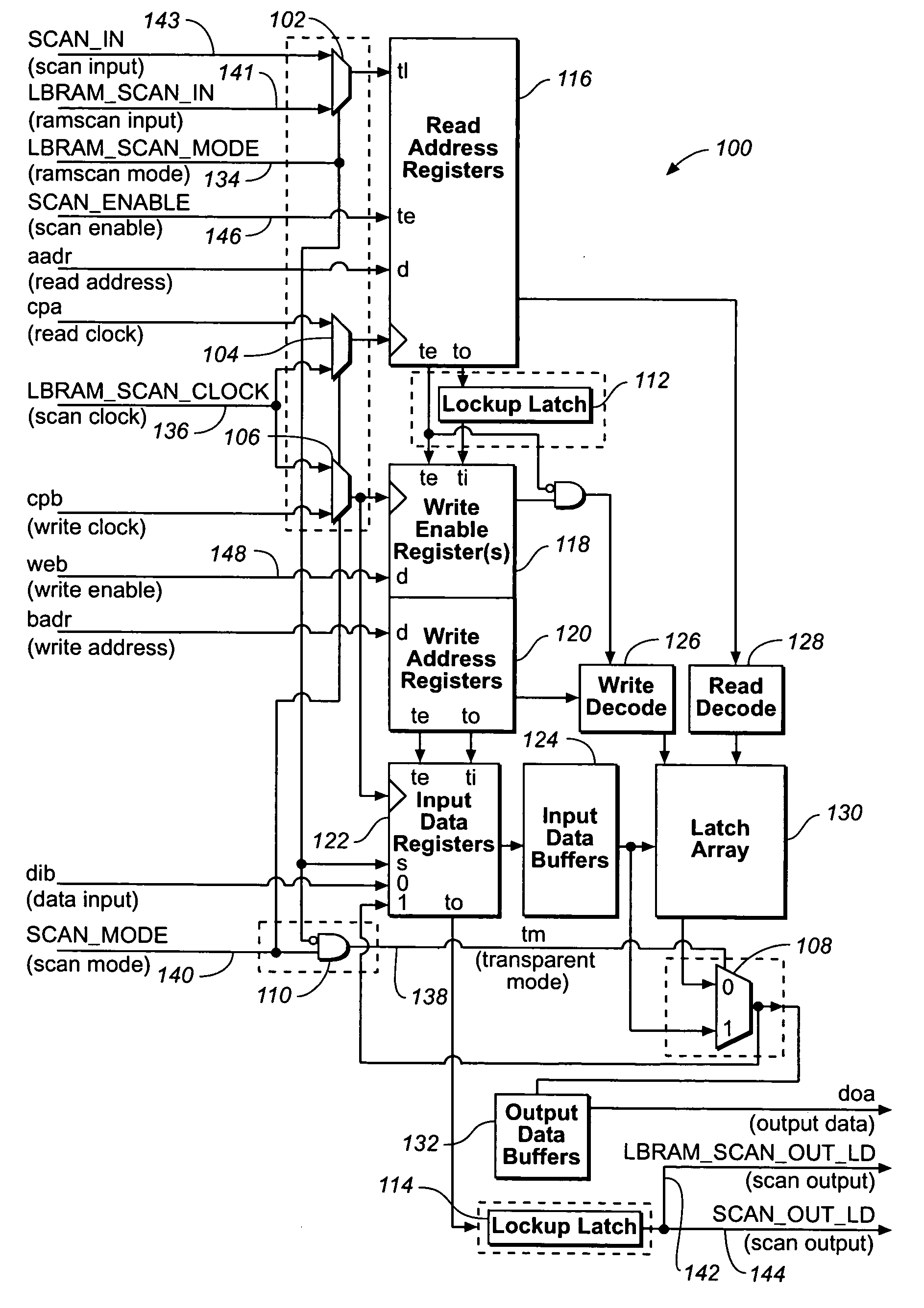
[0033] To facilitate testing of ASICs using automated test equipment (ATE), test logic is generally included in the ASIC circuit itself. The test logic usually functions only during testing and has no utility during normal operation of the ASIC in the field. Nevertheless, the test logic consumes additional die area in the ASIC, which results in fewer die manufactured on each wafer. The reduced wafer yield results in increased production costs. The automated test equipment is also expensive, consequently the testing time required for each ASIC further increases production costs.

[0034] As the use of latch based memory arrays in ASICS increases, there is an increased probability that faults will occur, necessitating more test logic. However, the added test logic for the memory arrays further increases the die area, disadvantageously reducing the wafer yield. Also, the additional testing required for more memory arrays increases the test time. To maintain high fault coverage without ex...


PUM


Abstract

A method and apparatus for testing latch based random access memory includes steps of generating a scan enable signal for testing latch based random access memory and generating a scan clock signal for testing the latch based random access memory wherein the scan clock signal has a first scan clock period for a shift cycle and a second scan clock period for a capture cycle.

Description

CROSS REFERENCE TO RELATED APPLICATIONS [0001] This application for patent claims the benefit of U.S. Provisional application No. 60 / 574,810, filed on May 26, 2004, for METHOD AND CIRCUIT FOR SCAN TESTING LATCH BASED RANDOM ACCESS MEMORY, incorporated herein by reference.BACKGROUND OF THE INVENTION [0002] 1. Field of the Invention [0003] The present invention relates generally to the design and testing of memory arrays for integrated circuits. More specifically, but without limitation thereto, the present invention relates to the design and testing of latch based random access memory (LBRAM) in an application-specific integrated circuit (ASIC). [0004] 2. Description of Related Art [0005] The use of memory arrays in application-specific integrated circuits (ASICs) is increasing, and it is estimated that memory arrays will constitute 94 percent of the die area in the average application-specific integrated circuit by the year 2014. There is also an increase in the use of small memorie...

Claims


Application Information

Patent Timeline
Patent Type & Authority Applications(United States)
IPC IPC(8): G11C29/00G11C29/32
CPCG11C11/41G11C2029/3202G11C29/32G11C29/1201
Inventor VINKE, DAVIDBALAJI, EKAMBARAM
Owner AVAGO TECH WIRELESS IP SINGAPORE PTE
Why Eureka
Try Eureka