Differential communication link with skew compensation circuit

a communication link and compensation circuit technology, applied in the field of differential signal skew correction circuits, can solve the problems of increasing the size, complexity, cost of the circuit board, and the design methods of the computer-based circuit board design tools that do not employ these design methods, so as to minimize the relative skew, reduce the reflection of signals, and minimize the effect of skew

Active Publication Date: 2012-01-31
MAYO FOUND FOR MEDICAL EDUCATION & RES
View PDF17 Cites 10 Cited by
  • Summary
  • Abstract
  • Description
  • Claims
  • Application Information

AI Technical Summary

Benefits of technology

[0023]In accordance with another aspect of the present invention, a method of minimizing skew in a high speed communication link includes terminating a differential signal having complementary positive and negative components received from a pair of transmission lines to reduce signal reflections, directing the terminated differential signal to a skew compensation circuit calculating a relative skew between the positive and negative components of the differential signal, directing a signal representative of the calculated skew to a controller, and generating output signals for at least one of the positive and negative components of the differential signal to minimize the relative skew therebetween.

Problems solved by technology

Because the dielectric constant of glass is typically higher, or at least different, than the surrounding resin, differential traces routed over such a glass weave structure typically exhibit a measurable amount of trace-to-trace variations in characteristic impedance and propagation delay, thus causing differential signal skew.
Currently, no known computer-based circuit board design tools employ these design methods to prevent differential signal skew caused by the weave effect.
Several of these design methods, such as non-orthogonal and disjoint routing techniques, are likely to require additional routing space, increasing the size, complexity, and cost of the circuit board.
Even after these methods become automated and common in high speed communication circuit boards, differential signal skew is also caused by other mechanisms including, for example, imbalanced trace routing, vias, connectors, return paths, and active circuitry.
Using these methods to minimize differential signal skew caused by the weave effect does not alleviate the skew-causing effects of these other mechanisms, and therefore are necessarily limited in application and value.
These methods do nothing to improve the integrity, enhance the value, or actually adjust the differential signal skew of the P and N sides within differential signals themselves.
Accordingly, these references do not provide a method of adaptively compensating for differential signal skew.
Still other design methods, believed to be suitable for their intended purposes, do not provide adequate correction of differential signal skew.
Due to losses in PCB interconnect products (i.e., up to 30 dB for a one-way loss and up to 60 dB [1000:1 voltage reduction] for a round-trip loss), the reflected signal strength can be drastically reduced, thus severely impacting the effectiveness of the internal feedback loop.
However, intermediate structures such as solder balls, connectors, and vias, present larger reflected signals back to the transmitter, thus further reducing the effectiveness of this method.
However, each of these methods sample the P and N sides independently using analog-to-digital (A / D) converters, thus eliminating the benefits of using differential signals.
As such, these methods do nothing to enhance the actual differential signal at the input to the receiver, but simply improve the displayed waveforms.
As such, the benefits of differential signal protocols are lost.
Also, the differential signal skew compensation is adjusted instantaneously for each and every signal transition, which can severely impact jitter and duty cycle distortion; thus, degrading the resulting differential signal.
However, this method cannot compensate for dynamic causes such as power droop or intersymbol interference.
Also, using training patterns is not always feasible in communication links, and the compensation adjustments are dependent on the data pattern.
As described above, this negates the benefits of using differential signals.
To be effective, the reconstructed signal needs to be converted to a digital format and then back to the analog domain within a fraction of the signal's edge rate, which severely limits the maximum data rate with which the method can be used.
In addition, the described “delay block” does not directly adjust the delay of the incoming analog signal, but instead performs a complex filtering function on the individual P and N sides of the differential signal, which again reduces the benefits of using differential signals.

Method used


Image

  • Differential communication link with skew compensation circuit
  • Differential communication link with skew compensation circuit
  • Differential communication link with skew compensation circuit

Examples


first embodiment

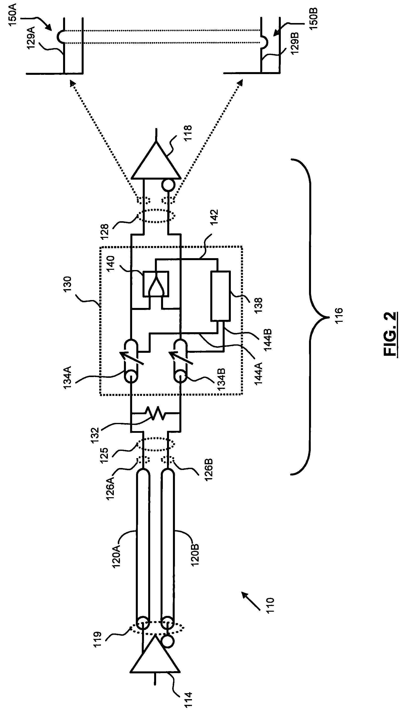
[0029]A high-speed differential signal communication link 110 according to the present invention is shown in FIG. 2. The communication link 110 includes a skew compensation circuit 130 disposed between a terminator 132 and a conventional differential signal receiver 118. A differential signal 119 generated by a conventional transmitter 114 is broadcast over a pair of differential transmission lines 120A, B in accordance with known systems and methods. The transmission lines 120A, B are terminated at the terminator 132 disposed in the receive end 116 of the link 110 to reduce signal reflections. Terminator 132 is shown as a single resistive element in FIG. 2, but those skilled in the art will recognize that transmission-line terminators can take many forms. The use of the term “terminator” is used herein to represent a circuit applied to the receive end 116 of a communication link 110 to provide optimal impedance match for minimizing signal reflections and / or optimizing the effective...

second embodiment

[0037]Turning now to FIG. 3, a high-speed differential signal communication link 210 according to the present invention is shown. The link 210 includes a skew compensation circuit 230 disposed between differential transmission lines 220A, B and a terminator 232. The configuration and operation of the skew compensation circuit 230 is similar to the circuit 130 of FIG. 2. The comparator skew detector 240, controller 238, and the delay elements 234A, B all operate in the same manner. However, the skew compensation circuit 230 is disposed upstream from a terminator 232 such that the effective input differential-impedance match into the skew compensation circuit 230 is enhanced by ensuring the received P-side and N-side signals 229A, B arrive simultaneously at the terminator, further improving the integrity of the differential signals 225.

third embodiment

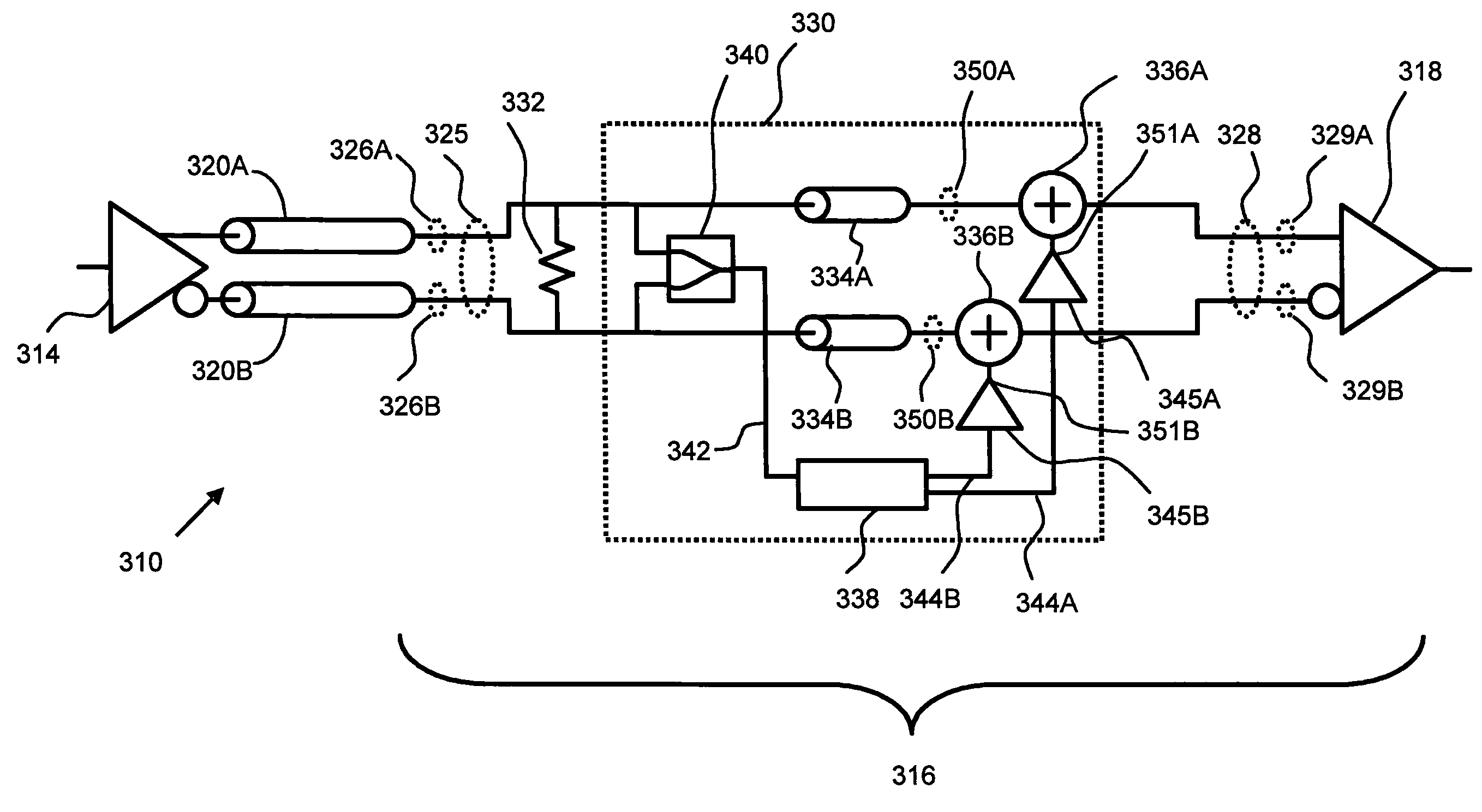
[0038]Turning now to FIG. 4, a high-speed differential signal communication link 310 according to the present invention is shown. Like the high speed communication link 110 of FIG. 2, a skew compensation circuit 330 is disposed between a terminator 332 and a differential signal receiver 318. Unlike the links 110, 210 of FIGS. 2 and 3, no variable-delay elements are used in the skew compensation circuit 330 to compensate for skew in the differential signal.

[0039]As illustrated, the differential transmission lines 320A, B are terminated at the terminator 332 directed into the skew-compensation circuit 330. The circuit 330 is configured to detect and reduce relative skew occurring between the P-side and N-side signals 329A, B of the differential signal 328 that are subsequently fed into the differential receiver 318 at the receive end 316 of the link 310.

[0040]The skew detector 340 monitors the P-side and N-side signals 326A, B of the received differential signal 325 and quantifies the...


PUM


Abstract

A system and method is presented for reducing skew between the positive and negative components of a differential signal in a high speed communications link. The communications link includes a signal generator producing and transmitting complementary positive and negative signals over separate transmission lines and a receiver receiving the complementary signals. The communication link further includes a skew compensation circuit having a skew detector, a controller, and separate delay and buffer elements for both the positive and negative component of the differential signal. The controller separately controls each of the delay or buffer elements in response to the detected skew between differential signal components.

Description

CROSS-REFERENCE TO RELATED APPLICATIONS[0001]This application is based on U.S. Provisional Patent Application Ser. No. 61 / 019,716, filed on Jan. 8, 2008, and entitled “DIFFERENTIAL SKEW-COMPENSATION CIRCUIT”, the contents of which are fully incorporated herein by reference.STATEMENT REGARDING FEDERALLY SPONSORED RESEARCH[0002]Not applicable.BACKGROUND[0003]1. Field of the Invention[0004]The invention relates generally to skew correcting circuits for differential signals and, in particular, to circuits for high-speed differential communication links that can measure and adaptively compensate for differential signal skew.[0005]2. Description of Related Art[0006]Today's high-speed communication systems often rely on differential signal protocols to enhance noise immunity, reduce transient currents, and increase effective signal amplitude. As depicted in FIG. 1, a conventional differential communication link 10 includes a transmit end 12 having a transmitter 14, a receive end 16 having ...

Claims


Application Information

Patent Timeline
Patent Type & Authority Patents(United States)
IPC IPC(8): G06F1/04
CPCH03L7/00H04L25/0272H04L25/03885H04L25/0298
Inventor ZABINSKI, PATRICK J.
Owner MAYO FOUND FOR MEDICAL EDUCATION & RES
Why Eureka
Try Eureka