Image pickup device

a pickup device and image technology, applied in the direction of radiation control devices, semiconductor devices, electrical devices, etc., can solve the problems of deterioration of blooming phenomena or color mixture, increase of dark current, and increase of charges leaked from adjacent pixels

Inactive Publication Date: 2005-12-08
CANON KK
View PDF11 Cites 110 Cited by
  • Summary
  • Abstract
  • Description
  • Claims
  • Application Information

AI Technical Summary

Benefits of technology

[0018] a first-conductivity-type fourth semiconductor region having an impurity concentration higher than the impurity concentration of the first semiconductor region is formed between the photoelectric conversion unit and the third semiconductor region and a first-conductivity-type fifth semiconductor region having an impurity concentration higher than the first semiconductor region is arranged between the photoelectric conversion unit and the third semiconductor region and arranged deeper than fourth semiconductor region.

Problems solved by technology

However, even by forming the channel stop region, when deepening a concentration profile of a PWL and using a PWL structure for improving a quantum efficiency of photoelectric conversion by a PD, a new technical problem is found that a dark current increases.
Moreover, when a well is deepened, a problem further occurs that the number of charges leaked from adjacent pixels increases.
Specifically, a problem of deterioration of a blooming phenomenon or color mixture occurs.

Method used


Image

  • Image pickup device
  • Image pickup device
  • Image pickup device

Examples


embodiment 1

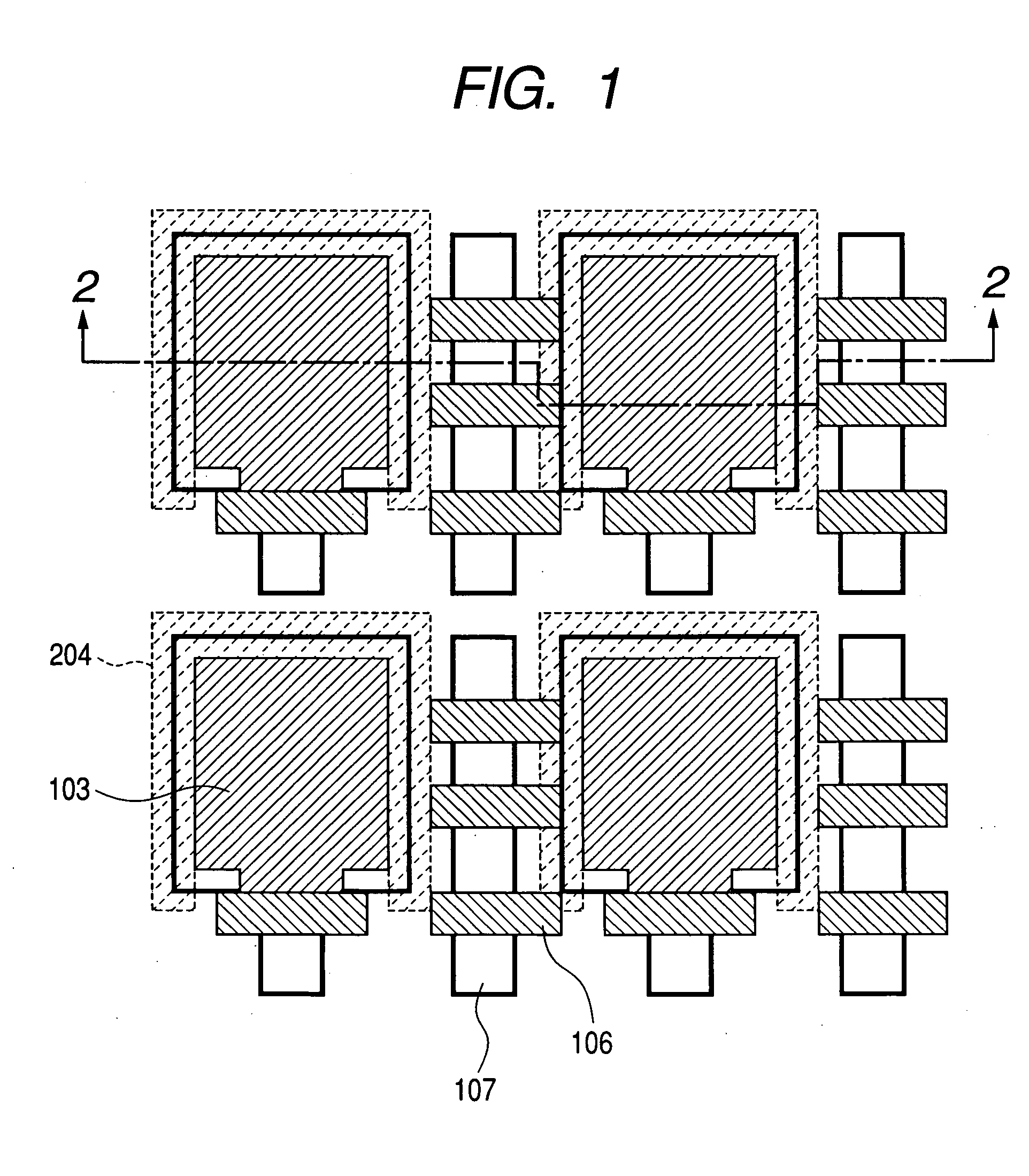
[0044]FIG. 1 is a top layout view of pixels of the image pickup device of the Embodiment 1 of the present invention.

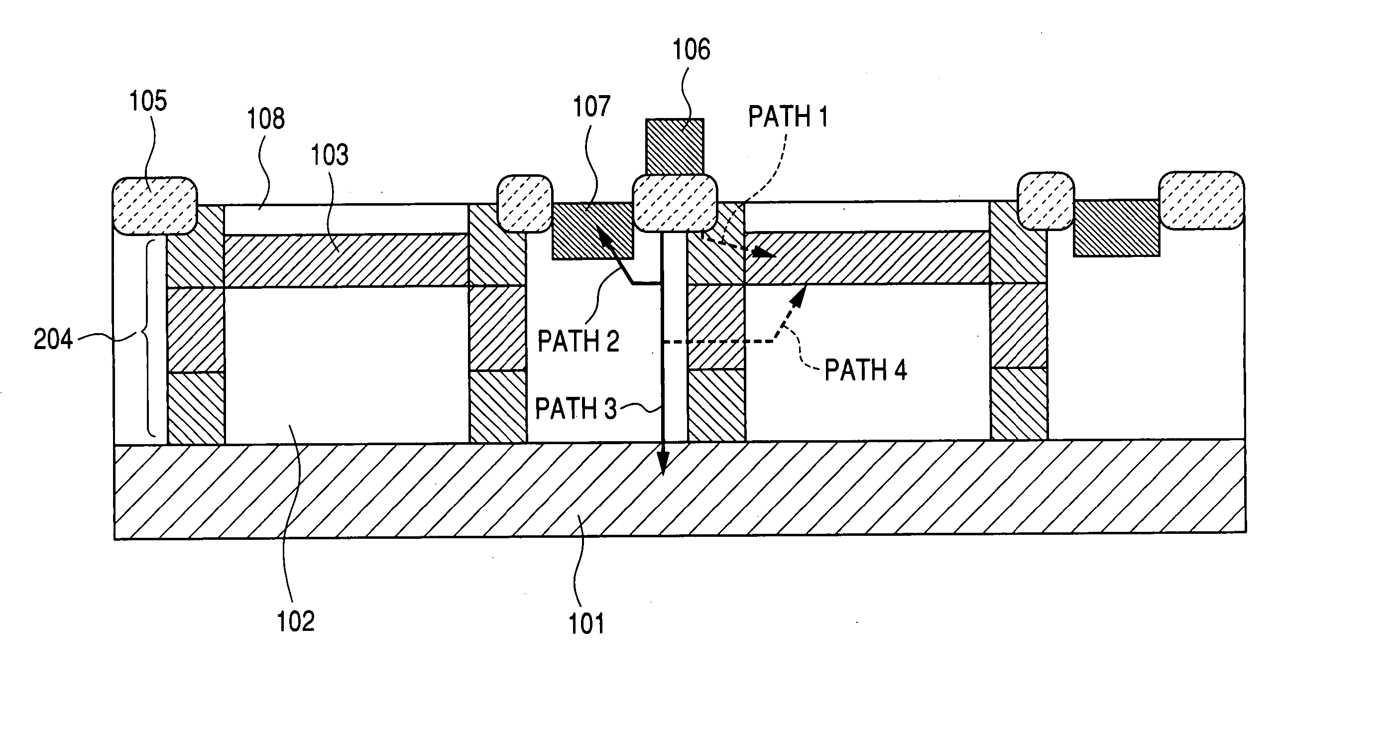
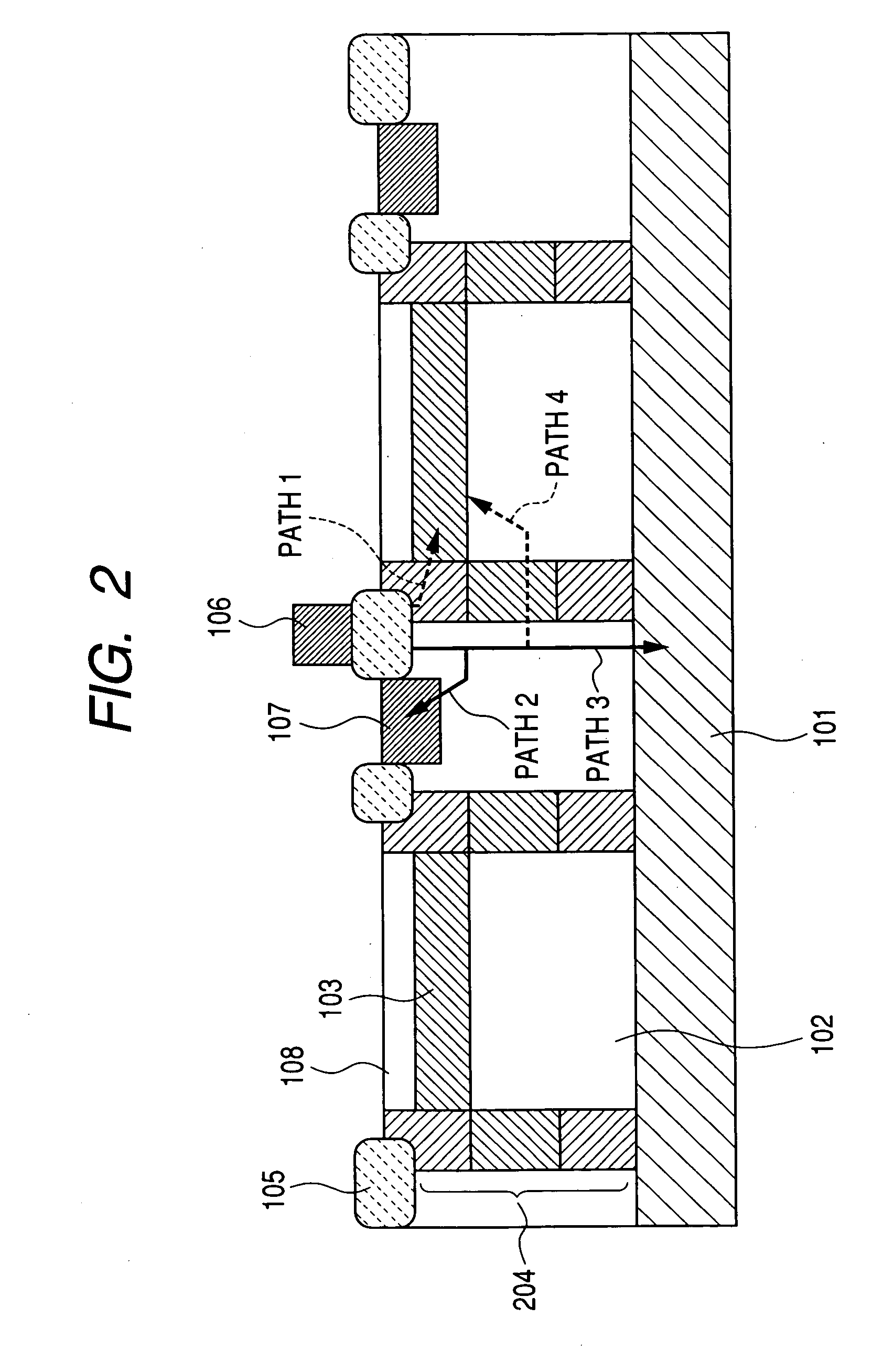
[0045]FIG. 2 is a sectional structural view along the line 2-2 in FIG. 1.

[0046] In FIG. 2, reference numeral 204 denotes a P-type semiconductor region (P+ guard layer) peculiar to the Embodiment 1.

[0047] As shown in FIG. 2, the present invention greatly decreases the dark current in accordance with a model for generating the dark current by using the following structure. As such configuration, (1) the P-type semiconductor region 204 is made to extend up to a position nearby the N-type substrate 101. Moreover, it is allowed to use a structure including at least a second P-type semiconductor region 204-2 at a position deeper than a first P-type semiconductor region 204-1. Furthermore, it is allowed to include a third P-type semiconductor region 204-3.

[0048] Furthermore, a configuration is used in which (2) the N+ region 107 is formed between the semiconductor region ...

embodiment 2

[0058]FIG. 3 is a sectional structural view of a pixel of an image pickup device of Embodiment 2.

[0059] The structure shown in FIG. 3 has a P-type semiconductor region 304-1 set over the lower portion of a MOS transistor in an adjacent photoelectric conversion unit under a P-type semiconductor region 304. In the case of the P-type semiconductor region 304-1, a concentration is set separately from the well of the MOS transistor and it is possible to form a high concentration barrier (potential barrier). It is possible to accelerate discharge of a few charges exceeding the concentration barrier (potential barrier) to the N+ region 107 and further restrain the charges from leaking into adjacent pixels by optimizing the concentration profile of the P-type semiconductor region 304-1.

embodiment 3

[0060]FIG. 4 is a top layout view of pixels of an image pickup device of Embodiment 3.

[0061] As shown in FIG. 4, by forming a P-type semiconductor region 404 into an annular shape and setting the region so that a photoelectric conversion unit and charge voltage conversion unit (FD) are included in the region, it is possible to provide an image pickup device in which dark current, blooming and color mixture are further restrained.

[0062]FIG. 5 is an illustration showing paths generated due to dark current, color mixture and blooming.

[0063] As shown in FIG. 5, when setting a P-type semiconductor region 504 as described above, paths 4-1 and 6-1 are left and a slight dark current, blooming and color mixture are left. However, by using the structure shown in FIG. 4, the paths 4-1 and 6-1 are restrained by the P-type semiconductor region 404 and it is possible to use the structure as a discharge destination of excessive charges and dark-current charges by setting a charge voltage conver...


PUM


Abstract

The present invention uses an image pickup device comprising a plurality of pixels respectively including a photoelectric conversion unit for converting incoming light into a signal charge, an amplifying unit for amplifying the signal charge generated by the photoelectric conversion unit and a transfer unit for transferring the signal charge from the photoelectric conversion unit to the amplifying unit, in which the photoelectric conversion unit is formed of a first-conductivity-type first semiconductor region and a second-conductivity-type second semiconductor region and a second-conductivity-type third semiconductor region is formed on at least a part of the gap between a photoelectric conversion unit of a first pixel and a photoelectric conversion unit of a second pixel adjacent to the first pixel, a first-conductivity-type fourth semiconductor region having an impurity concentration higher than that of the first semiconductor region is formed between the photoelectric conversion unit and the third semiconductor region and a first-conductivity-type fifth semiconductor region formed at a position deeper than the fourth semiconductor region and having an impurity concentration higher than that of the first semiconductor region is included between the photoelectric conversion unit and the third semiconductor region.

Description

BACKGROUND OF THE INVENTION [0001] 1. Field of the Invention [0002] The present invention relates to an image pickup device for converting an image to an electrical signal, and more particularly, to an active pixel sensor (hereafter referred to as APS) having an amplifier for each pixel or several pixels. [0003] 2. Related Background Art [0004] An image pickup device serving as an APS is also referred to as a CMOS sensor and widely used for digital cameras. This conventional image pickup device is described below by referring to FIGS. 9 to 12. [0005]FIG. 9 is a top layout drawing pf pixels of a conventional image pickup device. [0006]FIG. 10 is a cross-sectional structural drawing along the line 10-10 in FIG. 9. [0007]FIG. 11 is a concentration profile along the line Y-Y in FIG. 10. [0008]FIG. 12 is an equivalent circuit diagram using the image pickup device in FIG. 9. [0009] In FIG. 12, reference numeral 121 denotes a photodiode (PD) for converting light into a signal charge and 12...

Claims


Application Information

Patent Timeline
Patent Type & Authority Applications(United States)
IPC IPC(8): H01L27/146H01L31/0352
CPCH01L27/14603H01L27/14609H01L27/14641H01L31/03529H01L31/035281
Inventor KOIZUMI, TORUSAKAI, SEIICHIROOGURA, MASANORI
Owner CANON KK
Why Eureka
Try Eureka