Semiconductor device

a technology of semiconductor devices and semiconductors, applied in semiconductor devices, semiconductor/solid-state device details, electrical apparatus, etc., can solve the problems of increasing the area (size) of the substrate, increasing the manufacturing cost of the substrate, and difficult to form high-density wiring on the low-cost substrate. , to achieve the effect of low cost, high accuracy and fine structur

US20050269701A1Inactive Publication Date: 2005-12-08SOCIONEXT INC
4 Cites 8 Cited by

Patent Information

Authority / Receiving Office
US · United States
Patent Type
Applications(United States)
Current Assignee / Owner
Publication Date
2005-12-08
Estimated Expiration
Not applicable · inactive patent

Smart Images

  • Figure 1
    Figure 1
  • Figure 2
    Figure 2
  • Figure 3
    Figure 3
Patent Text Reader

Abstract

In a semiconductor device, bonding-wires can be applied parallel to each other to electrodes of high-speed signal lines when mounting a highly densified semiconductor element on a low-cost substrate while reducing a length of the bonding-wires. An impedance-matched substrate having wiring that impedance-matched with circuits of a semiconductor element is mounted on a substrate. A plurality of first metal wires connect between first electrodes of the semiconductor element and electrodes of the substrate. A plurality of second metal wires connect between second electrodes of the semiconductor element and first electrodes of the impedance-matched substrate. A plurality of third metal wires connect between second electrodes of the impedance-matched substrate and electrodes of the substrate. The second metal wires extend parallel to each other, and the third metal wires also extend parallel to each other.
Need to check novelty before this filing date? Find Prior Art

Description

BACKGROUND OF THE INVENTION

[0001] 1. Field of the Invention

[0002] The present invention relates to semiconductor devices and, more particularly, to a semiconductor device in which a semiconductor element is mounted on a substrate by wire-bonding.

[0003] 2. Description of the Related Art

[0004] In recent years, high-densification of semiconductor element has progressed, which causes a reduction in a pitch of electrode terminals formed on an semiconductor element. Additionally, a processing speed of input and output signals has been increased, which results in, in many cases, provision of electrode terminals for inputting and outputting high-frequency signals.

[0005] High-frequency signal lines connected to the electrode terminals for outputting and inputting high frequency signals need to take impedance-matching with peripheral circuits and wirings. Generally, a differential pair is formed by two high-frequency lines, and the differential pair is located between shielding lines suc...

Examples

Embodiment Construction

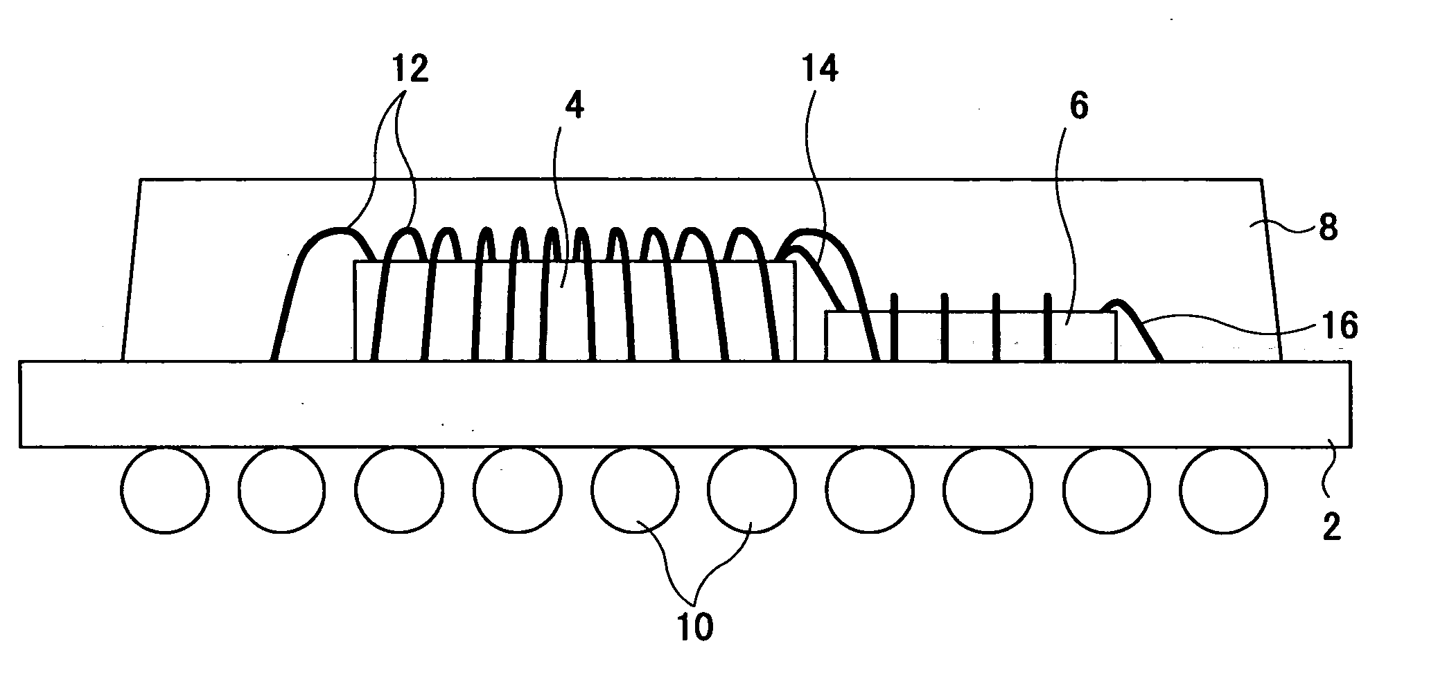
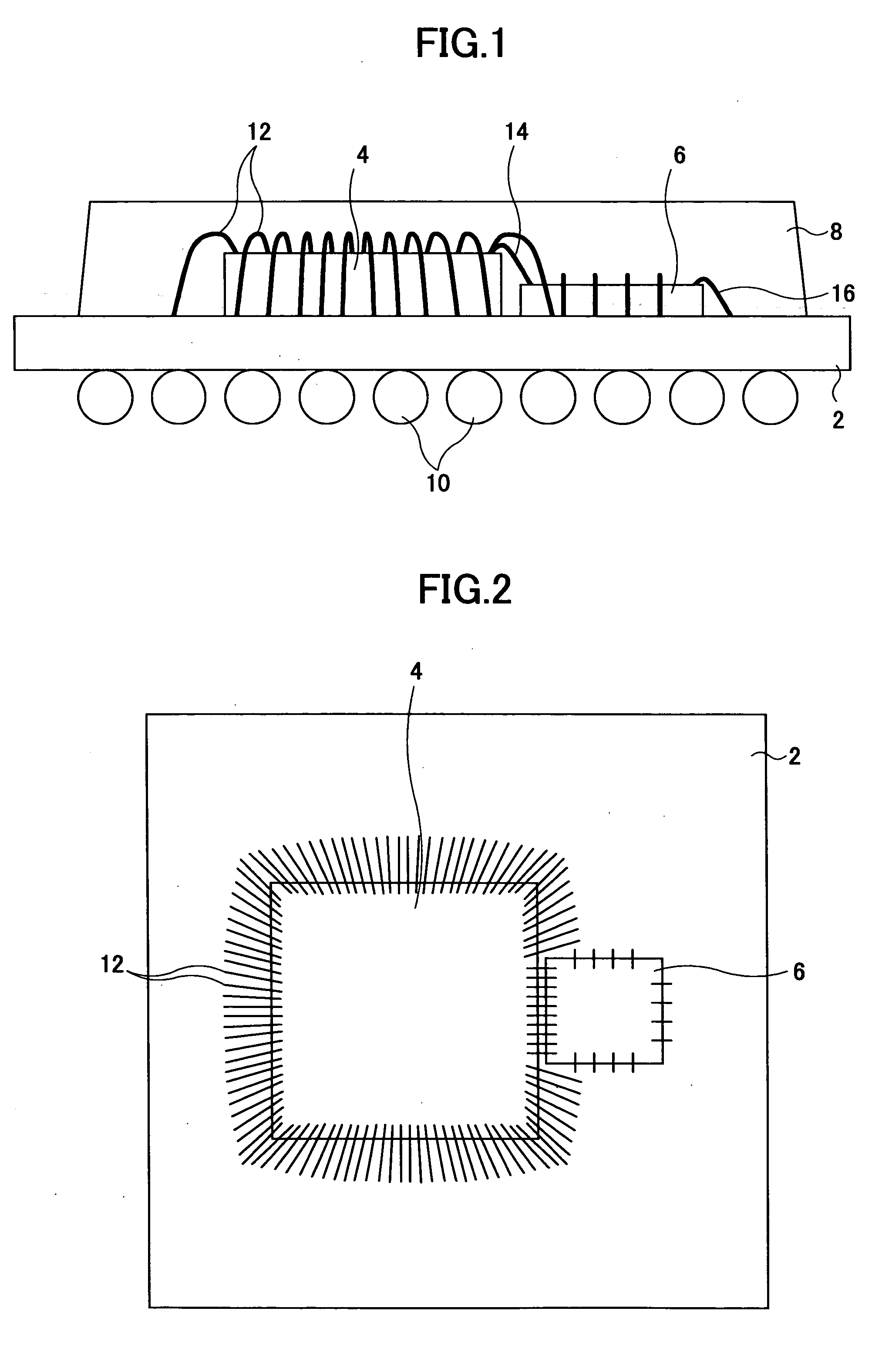
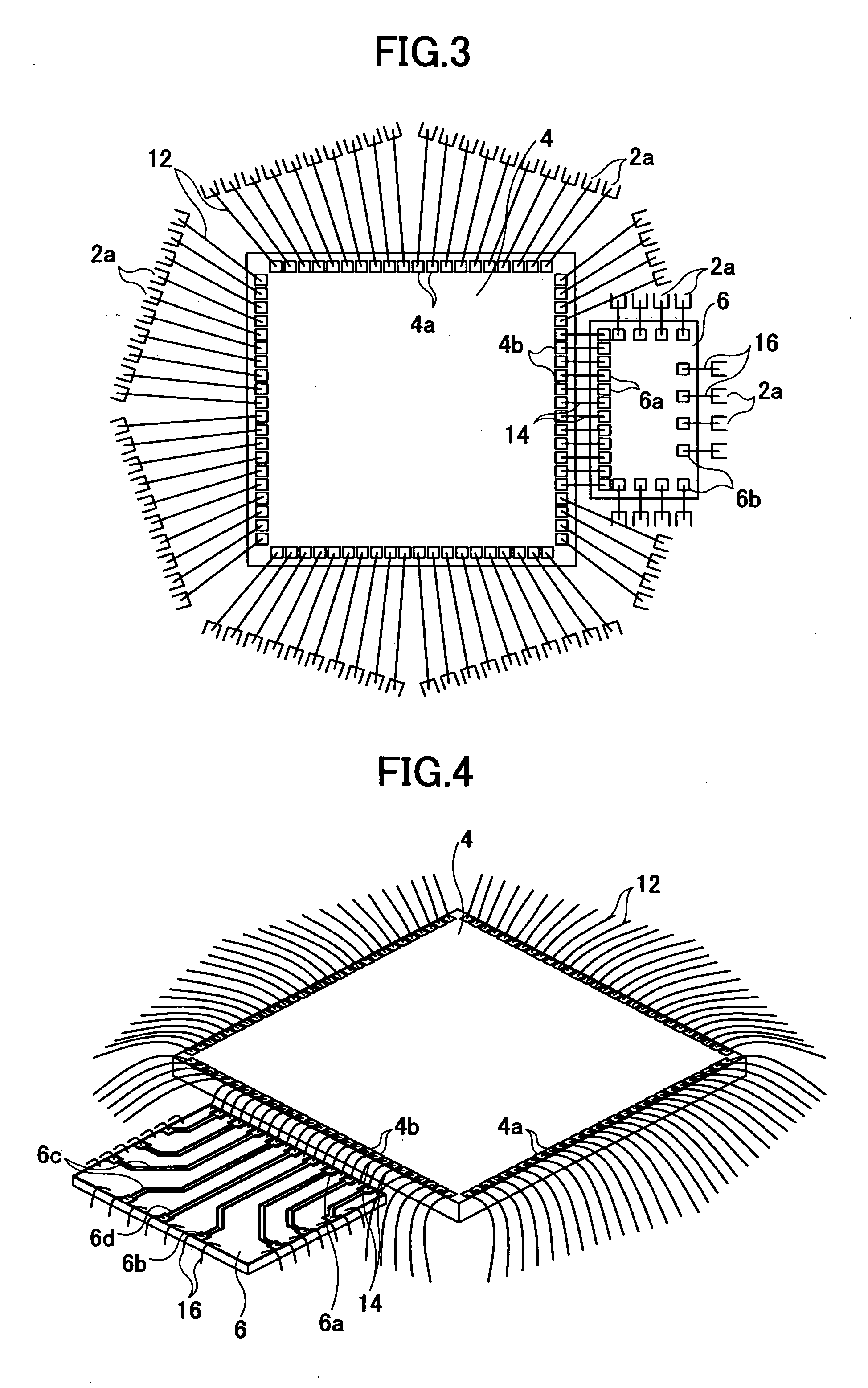
[0037] A description will now be given, with reference to FIGS. 1 through 3, of a semiconductor device according to a first embodiment of the present invention. FIG. 1 is an internal a see-through side view of a ball-grid array (BGA) type semiconductor device according to the first embodiment of the present invention. FIG. 2 is a see-through plan of the semiconductor device shown in FIG. 1. FIG. 3 is a plan view showing a structure of bonding-wires in the semiconductor device shown in FIG. 1.

[0038] The semiconductor device according to the first embodiment of the present invention comprises a substrate 2, a semiconductor element 4 mounted on the substrate 2 and an impedance-matched substrate 6 mounted on the substrate 2. The semiconductor element 4 and the impedance-matched substrate 6 are wire-bonded to electrodes 2a (refer to FIG. 3) of the substrate 2, and those are entirely encapsulated by a seal resin 8 on the substrate 2. Provided on the backside of the substrate 2 are solder...