Solid-state image pickup device and camera

a pickup device and solid-state technology, applied in the field of solid-state image pickup devices, can solve the problem of increasing the size of the adder circuit, and achieve the effect of suppressing random noise of the photoreceiving elements

Active Publication Date: 2005-12-08
CANON KK
View PDF8 Cites 32 Cited by
  • Summary
  • Abstract
  • Description
  • Claims
  • Application Information

AI Technical Summary

Benefits of technology

[0016] According to the invention, the random noises of the photoreceiving elements can be suppressed by adding and averaging the signals. In dependence on a type of photoreceivin

Problems solved by technology

There is, consequently, such a problem that the more a number of addition pixels exist in the vertical directi

Method used


Image

  • Solid-state image pickup device and camera
  • Solid-state image pickup device and camera
  • Solid-state image pickup device and camera

Examples


reference example 1

[0032]FIG. 7 shows the first reference example regarding the invention. This reference example shows an example of a case of executing a signal addition (averaging) of (3 pixels in the horizontal direction)×(3 pixels in the vertical direction) in a pixel array of (H columns×V rows).

[0033] In FIG. 7, reference numerals 101-a to 101-i denote photoreceiving elements which are two-dimensionally arranged. Reference numerals 112 to 114 denote-vertical output lines to which a photoreceiving element train constructed by the photoreceiving elements 101-a, 101-d, and 101-g, a photoreceiving element train constructed by the photoreceiving elements 101-b, 101-e, and 101-h, and a photoreceiving element train constructed by the photoreceiving elements 101-c, 101-f, and 101-i are connected, respectively. Reference numerals 102-a to 102-c denote clamp capacitors in which one terminal is connected to the vertical output lines 112 to 114 and the other terminals are connected in common. Signals of th...

reference example 2

[0041]FIG. 10 shows the second reference example of the invention. This reference example shows an example of a case of executing a signal addition of (3 pixels in the horizontal direction)×(4 pixels in the vertical direction) in a pixel array of (H columns×V rows).

[0042] In FIG. 10, reference numerals 401-a to 401-P denote photoreceiving elements which are two-dimensionally arranged. Reference numerals 413 to 415 denote vertical output lines. Reference numerals 402-a to 402-c denote clamp capacitors. The signal addition in the horizontal direction is executed by using those capacitors. Reference numeral 403 denotes an MOS switch for clamping which is connected to the clamp voltage Vclmp; 410 a common line for averaging outputs after the clamping; and 404 to 407 MOS switches for selecting the S / H capacitors. The MOS switches 404 to 407 are used to select the S / H capacitors. Reference numerals 408-a to 408-d denote sampling and holding capacitors and 409-a to 409-d indicate MOS swit...

embodiment 1

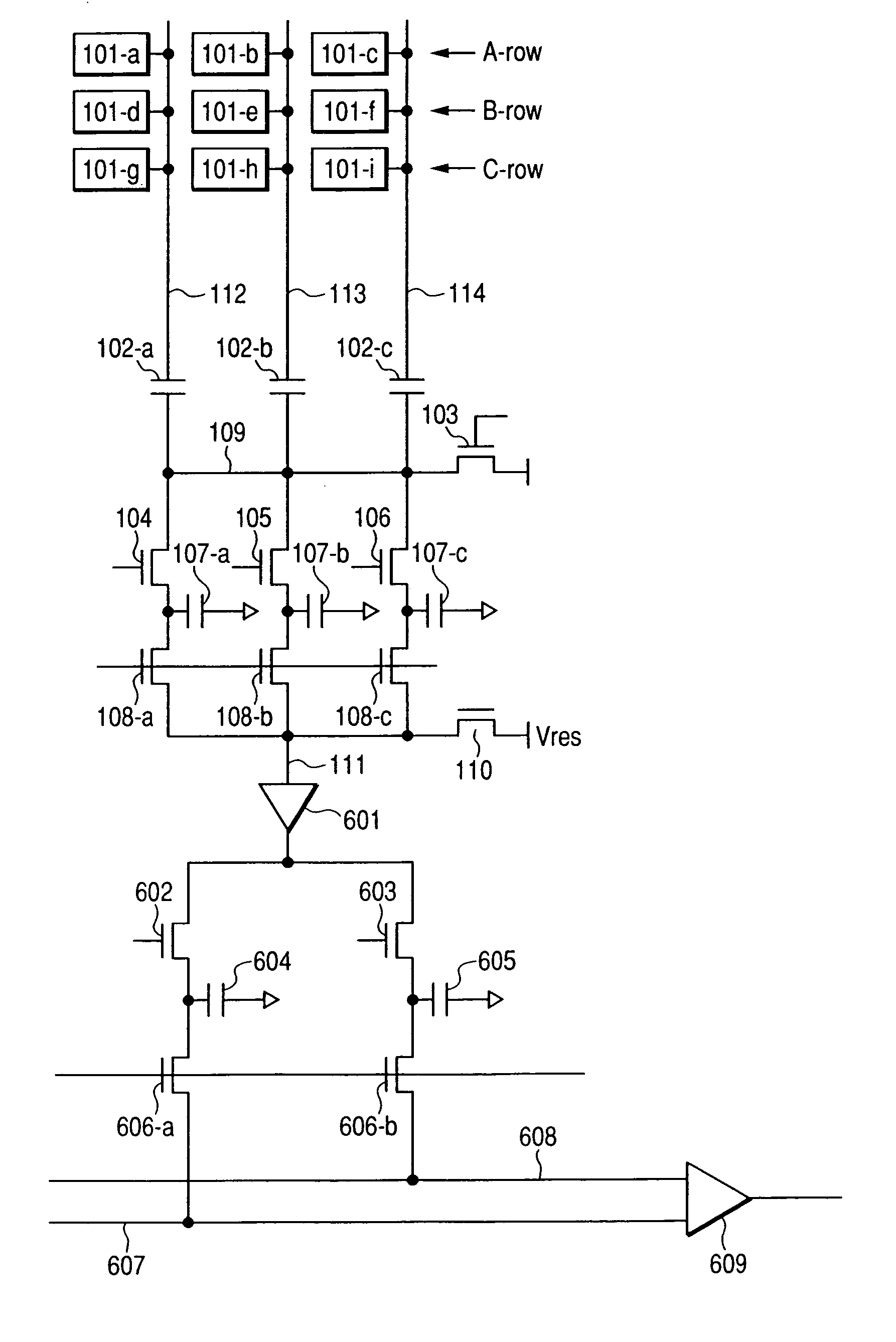
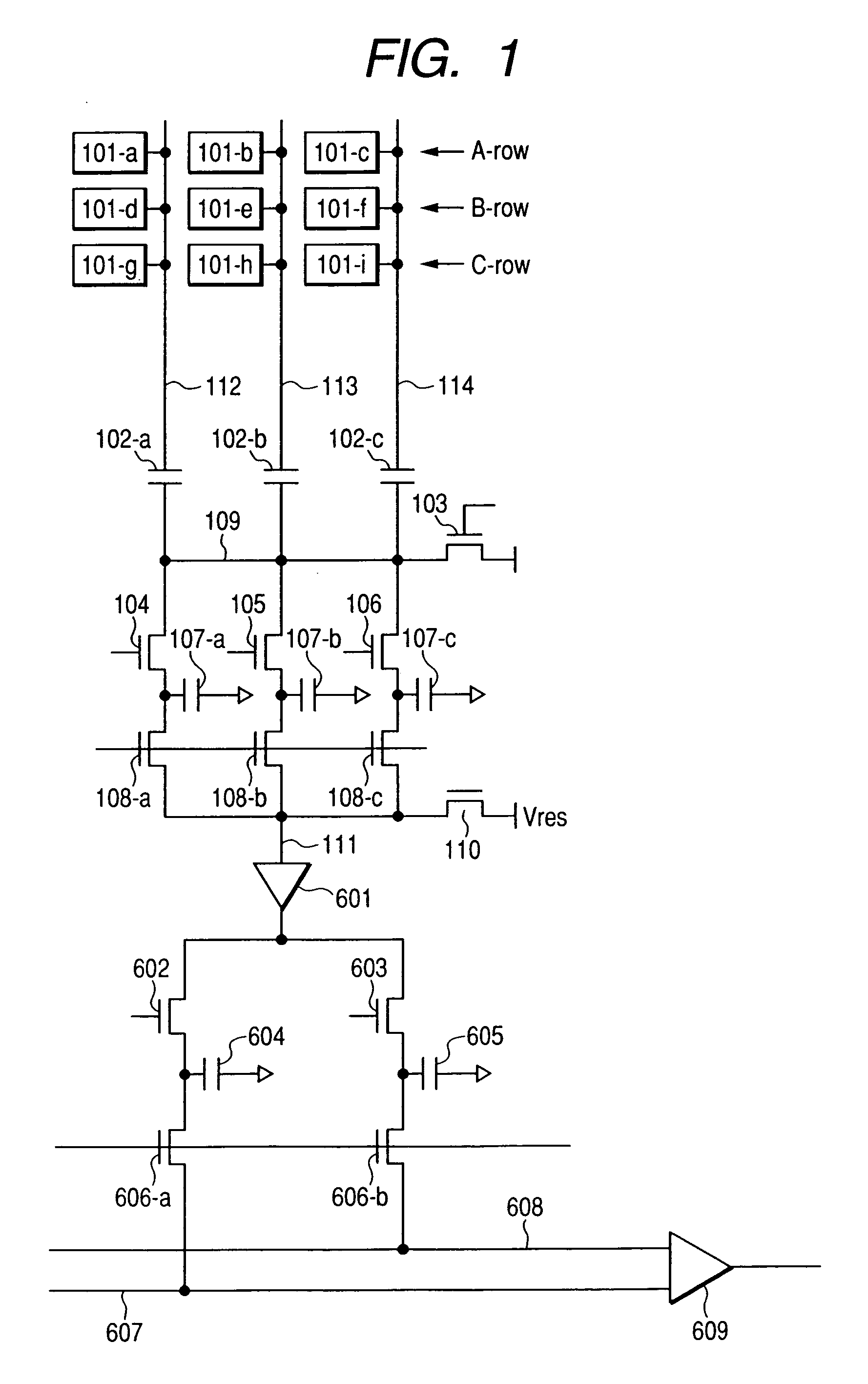
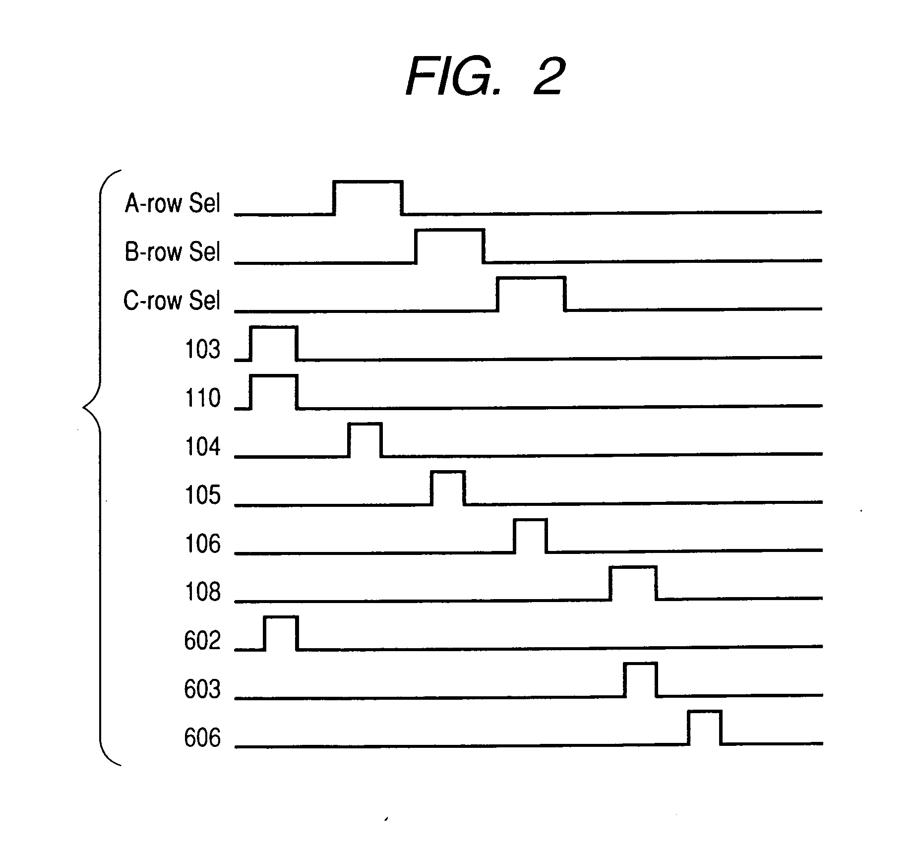
[0048]FIG. 1 shows the first embodiment according to the invention. This embodiment shows an example of the case of executing the addition of signals of (3 pixels in the horizontal direction)×(3 pixels in the vertical direction) in the pixel array of (H columns×V rows). By using this embodiment, loss of the signal components can be reduced more than that in the reference example 1. The same or similar component elements as those shown in FIG. 7 are designated by the same reference numerals and their description is omitted. Naturally, a construction of the embodiment can be also applied to the case of executing the addition of signals of (3 pixels in the horizontal direction)×(4 pixels in the vertical direction) in the pixel array of (H columns×V rows).

[0049] In FIG. 1, reference numeral 601 denotes a source follower amplifier; 602, 603, 606-a, and 606-b MOS switches; and 604 and 605 line memories. By turning on the MOS switch 602, a noise signal (containing an offset of the source ...


PUM


Abstract

The number of necessary sampling and holding capacitors is reduced. A solid-state image pickup device has signal lines to which photoreceiving elements are connected, a clamp circuit that has clamp capacitors in which one terminal is connected to the signal lines and the other terminals are short-circuited, has a switch for applying a reference voltage to the other terminals by the clamping operation, and adds signals from the plurality of photoreceiving elements provided in the row direction along with the clamping operation, adding means (switches and capacitors) which is connected to the other terminals of the clamp capacitors, adds addition signals of the respective photoreceiving element rows outputted from the other terminals and adds the signals of the plurality of photoreceiving elements provided in the column direction; an amplifier connected to the adding means; a switch for resetting the input side of the amplifier; and circuit means (switches and capacitors) for outputting an offset of the amplifier and the signal from the amplifier.

Description

BACKGROUND OF THE INVENTION [0001] 1. Field of the Invention [0002] The invention relates to a solid-state image pickup device having photoreceiving elements and, more particularly, to a solid-state image pickup device which can add signals from photoreceiving elements. [0003] 2. Related Background Art [0004] A number of solid-state image pickup devices in each of which pixels including photoelectric conversion units are one-dimensionally or two-dimensionally arranged are used in digital cameras, video cameras, copying apparatuses, facsimile apparatuses, and the like. As solid-state image pickup devices, there are an amplifying type solid-state image pickup device such as CCD image pickup device, CMOS image pickup device, and the like. [0005] In association with an increase in the number of pixels of an image sensor such as a solid-state image pickup device, in recent years, not only the conventional usage where signals of all pixels of the image sensor are always simply sequentiall...

Claims


Application Information

Patent Timeline
IPC IPC(8): H04N5/335H01L27/146H04N5/343H04N5/347H04N5/357H04N5/363H04N5/369H04N5/374H04N5/376H04N5/378H04N9/07H04N101/00
CPCH04N5/347H04N5/378H04N5/3742H04N5/3575H04N25/46H04N25/616H04N25/767H04N25/75
Inventor NODA, TOMOYUKIKIKUCHI, SHIN
Owner CANON KK
Why Eureka
Try Eureka