

Method for fabricating a self-aligned nanocolumnar airbridge and structure produced thereby
a nanocolumnar airbridge and self-alignment technology, which is applied in the manufacture of electrode systems, cold cathode manufacturing, electric discharge tubes/lamps, etc., can solve the problem of general requirement of harsh reactive ion etching processes on metallic lines
- Summary
- Abstract
- Description
- Claims
- Application Information
AI Technical Summary
Benefits of technology
Problems solved by technology
Method used
Image

Examples
Embodiment Construction
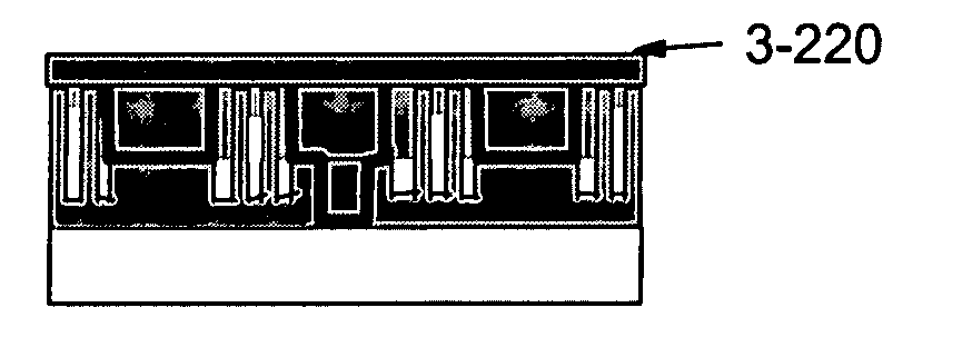
[0046] This invention relates to a variety of extreme low k interconnect structures including a conductor that is encased in a dielectric medium, is supported transversely by a bridge member extending to an adjacent interconnect line and is supported vertically by vias and a dielectric support that is either continuous or patterned to lie only under the metal lines. The regions between the adjacent conductor lines are occupied either by nanocolumnar voids in a dielectric or by pillars of dielectric.
[0047] In the method of the present invention for fabricating a low k, ultra-low k, and extreme-low k multilayer interconnect structure on a substrate, the interconnects are separated laterally by an ILD that has nanocolumnar air gaps. The structure has a support layer in the via level of a dual damascene structure that is only under the metal line and the effective dielectric constant of a dielectric is decreased by perforating it using sub-optical lithography patterning techniques.
[00...
PUM
 Abstract
Description
Claims
Application Information