Data transfer method and data transfer device

a data transfer and data technology, applied in the field of data transfer methods, can solve the problems of increasing the number of wiring and complication of wiring, increasing the number of signal lines, etc., to improve the transfer state of data, and reduce the speed of data transfer

Inactive Publication Date: 2005-12-08
CANON KK
View PDF8 Cites 38 Cited by
  • Summary
  • Abstract
  • Description
  • Claims
  • Application Information

AI Technical Summary

Benefits of technology

[0051] Preferably, the first and second slave chips have respective registers, and the data transfer step comprises transferring as the data information on writing in or reading from at least one of the slave chips, or on resetting of at least one of the slave chips.
[0052] Preferably, the first and second slave chips receive the data transferred from the master chip, the data being all handled as transactions in units of transactions each formed by several bits, analyze each received transaction, and complete processing of the transaction by carrying out internal processing, such as writing, reading, or resetting, on a register provided in the slave chip, or transferring the data as the transaction to a next one of the slave chips to finally transfer the data as the transaction to the master chip.
[0053] Preferably, the method comprises a storage step of storing a transfer state of the data transferred from the master chip to the first and second slave chips in the first and second slave chips.
[0054] More preferably, the transfer state of the data represents reliability of a signal line for transferring the data, dependent on noise superposed on the data being transferred along the signal line depending on a transfer condition of the data.
[0055] More preferably, the method comprises a reading step of causing the master chip to read the transfer state of the data stored in the first and second slave chips from the master chip, by a method selected from the group consisting of a first method of reading the transfer state of the data stored in the first and second slave chips in a same manner as reading from the registers provided in the first and second slave chips, and a second method of outputting information on the transfer state, from the first and second slave chips, using a signal line other than the signal line connecting between the first and second slave chips.
[0056] More preferably, the method comprises a reading step of causing the master chip to read the transfer state of the data stored in the first and second slave chips from the master chip, and a transfer speed lowering step of lowering a speed of transfer of the data when the read transfer state of the data is in an error condition, to thereby improve the transfer state of the data.

Problems solved by technology

Actually, however, signal lines of the buses are often used to connect the master chip and the slave chips, causing an increase in the number of lines of wiring and complication of the wiring.
This necessitates provision of as many resetting signal lines as the slave chips to be reset, which causes an increase in the number of lines of wiring and complication of the wiring.
Further, as many signal lines for the chip select signal as the slave chips are required, which results in an increase in the number of signal lines.
The master chip cannot know the state of a signal level of each signal line via which the data is transferred from the master chip to the associated slave chip, and there is a possibility that noise is added to the signal line depending on the conditions of the circuit board and the wiring conditions of the signal line, whereby the signal level is changed due to the influence of the noise, causing an error in transfer of the data.
In this case, depending on the setting of a parity bit, the processing can sometimes detect an error in the data, but the reliability of the processing is low.
More specifically, when communication by serial data is performed between the master chip and each slave chip, the slave chip determines an error condition of the serial data by parity check or the like, but depending on the bit position of an error, the error cannot be detected.
Further, even when it is configured such that an interruption is caused to occur based on a parity error, if the parity error occurs frequently, the performance of a control section, such as a CPU, connected to the slave chip can be degraded due to the control section being interrupted each time the parity error occurs.
In the case of the former method, an interruption signal is output from each slave chip to the master chip, and therefore it is necessary to provide as many interruption signal lines as the slave chips, which results in an increase in the number of signal lines and an increase in the number of pins.
Therefore, an error occurs in the data being transferred from the master chip to the slave chip, and when the same data is sent back to the master chip, an error is caused by the influence of noise superposed on the data.

Method used


Image

  • Data transfer method and data transfer device
  • Data transfer method and data transfer device
  • Data transfer method and data transfer device

Examples


first embodiment

[0092] First of all, a description will be given of the present invention with reference to FIGS. 1 to 7.

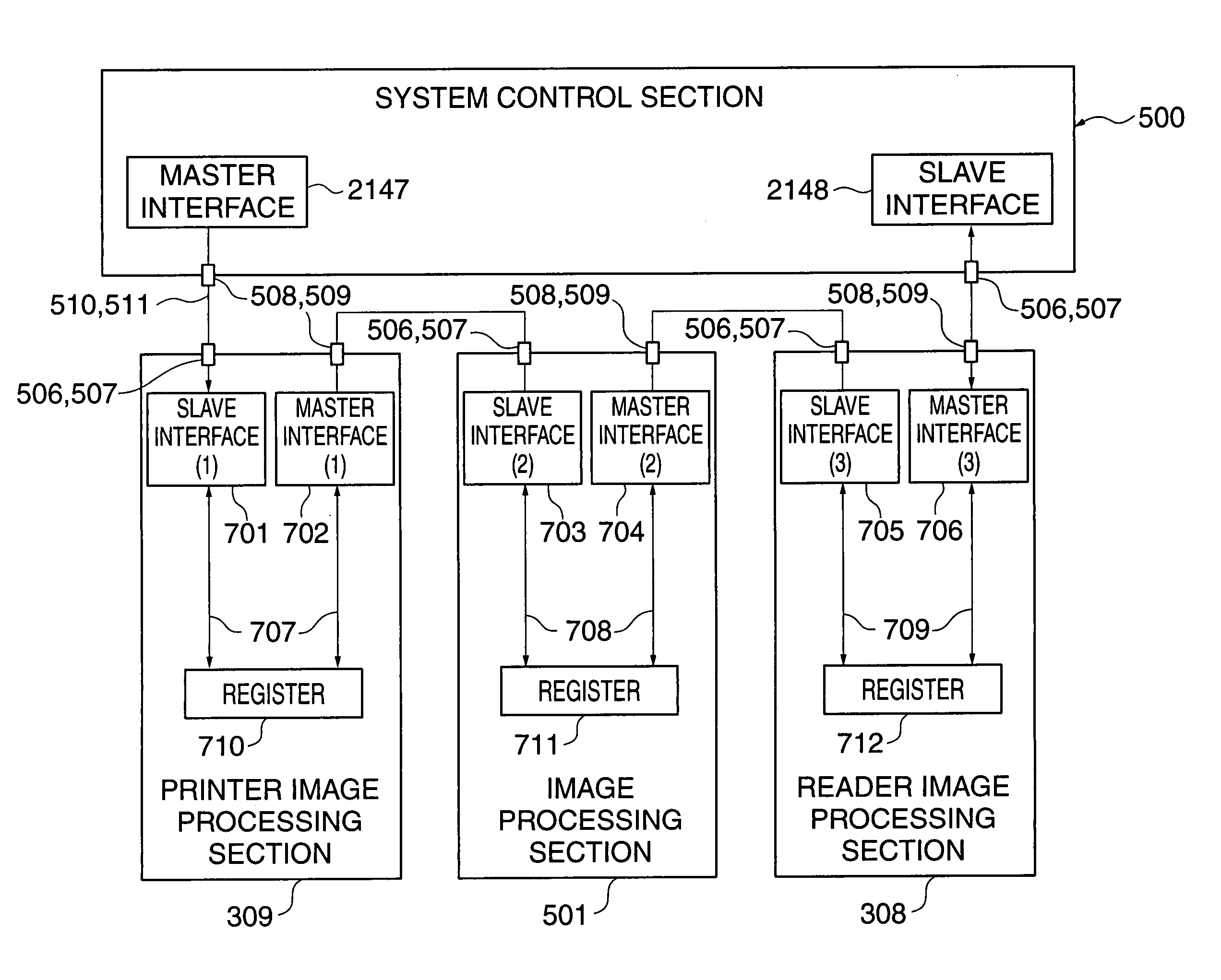
[0093] In the present embodiment, to solve the above-described problems with the prior art, two or more slave chips are connected in a ring to a single master chip by two signal lines, i.e. a serial data signal line and a transfer synchronizing clock line. It is configured such that on the serial data signal line information on register data is transferred and information on serial data on the serial data signal line is sequentially transferred from one slave chip to another, to finally return to the master chip.

[0094] Similarly to the serial data signal line, it is configured such that on the transfer synchronizing clock line a clock signal transmitted from the master chip is sequentially transferred from one slave chip to another, to finally return to the master chip.

[0095] The master chip and the slave chips receive and transmit the serial data on the serial data signal line...

second embodiment

[0192] Next, a description will be given of the present invention with reference to FIGS. 8 to 10.

[0193] In the present embodiment, similarly to the first embodiment, to solve the problems with the prior art, two or more slave chips are connected in a ring to a single master chip by two signal lines, i.e. a serial data signal line and a transfer synchronizing clock line such that register data to be transferred can be sent as serial data along the serial data signal line and transferred from one slave chip to another, to finally return to the master chip.

[0194] Similarly to the serial data transferred on the serial data line, the synchronizing clock signal flowing on the transfer synchronizing clock line can be transferred from one slave chip to another, to finally return to the master chip.

[0195] The master chip and the slave chips receive and transmit the serial data on the serial data signal line in timing synchronous with the synchronizing clock signal on the transfer synchron...

third embodiment

[0296] Next, a description will be given of the present invention.

[0297] In the present embodiment as well, to solve the problems with the prior art, two or more slave chips are connected in a ring to a single master chip by two signal lines, i.e. a serial data signal line and a transfer synchronizing clock line such that register data to be transferred can be sent as serial data along the serial data signal line and transferred from one slave chip to another, to finally return to the master chip.

[0298] Similarly to the serial data transferred on the serial data line, the synchronizing clock signal flowing on the transfer synchronizing clock line can be transferred from one slave chip to another, to finally return to the master chip.

[0299] The master chip and the slave chips receive and transmit the serial data on the serial data signal line in timing synchronous with the synchronizing clock signal on the transfer synchronizing clock line.

[0300] The serial data is transferred fro...


PUM


Abstract

A data transfer method which is capable of transferring a predetermined amount of data in one transaction at only one time, and preventing the number of ports of a master chip and the number of signal lines connected between the master chip and slave chips from being increased. A single master chip and a plurality of slave chips which receive data transferred from the master chip are connected by a ring-like path. Data is transferred from the master chip to the slave chips via the ring-like path.

Description

BACKGROUND OF THE INVENTION [0001] 1. Field of the Invention [0002] The present invention relates to a data transfer method of interconnecting electronic chips, such as IC chips, and a data transfer device. [0003] 2. Description of the Related Art [0004] To enable configuration or the like of registers of a plurality of slave chips to be performed between one master chip and the slave chips, the master chip is connected to the slave chips by respective signal lines of address buses, signal lines of writing data buses, signal lines of reading data buses, and chip-selecting signal lines, for configuration of the registers (see Japanese Laid-Open Patent Publication (Kokai) No. 2001-142735). [0005] Further, for resetting as well, reset pins are provided separately for the respective slave chips, and a plurality of signal lines for resetting signals are separately connected to the respective reset pins on a circuit board. [0006] In this case, all the signal lines of the buses and the res...

Claims


Application Information

Patent Timeline
Patent Type & Authority Applications(United States)
IPC IPC(8): G06T1/20G06F13/00G06F13/16G06F13/36G06F13/38G06F13/42
CPCG06F13/4256G06F13/14
Inventor YAMAMOTO, NAOHIRO
Owner CANON KK
Why Eureka
Try Eureka