Microfluidic device with electrode structures

a microfluidic device and electrode technology, applied in the direction of microstructural technology, diaphragms, electrodes, etc., to achieve the effect of identifying the ‘fingerprints’ of the electrodes and precise shaping of the electric fields

Inactive Publication Date: 2005-12-15
UNIV TECH INT
View PDF1 Cites 45 Cited by
  • Summary
  • Abstract
  • Description
  • Claims
  • Application Information

AI Technical Summary

Benefits of technology

[0004] This patent document discloses methods of generating electric fields in microfluidic devices, particularly those fabricated with channels in PDMS (polydimethylsiloxane). In one example, electrodes are embedded into the microfluidic channel system. In another example, posts, for example made from PDMS, are incorporated into microfluidic channels to allow precise shaping of electric fields. Field-shaping metal electrodes embedded in the PDMS-glass hybrid microchannels may be used to manipulate and isolate microscopic particles including biological cells and biomaterials (DNA, RNA, Proteins). The technique of fabricating microchannels using PDMS may be combined with Dielectrophoresis (DEP) for manipulating microscopic particles including biological cells and in successful identification of their DEP ‘fingerprints’.

Problems solved by technology

For over a decade, the realization of miniaturized laboratory functions onto a microchip capable of performing rapid chemical / biochemical analyses using very small inventories of samples and reagents has been a challenging goal for many leading research groups world wide.

Method used


Image

  • Microfluidic device with electrode structures
  • Microfluidic device with electrode structures
  • Microfluidic device with electrode structures

Examples


Embodiment Construction

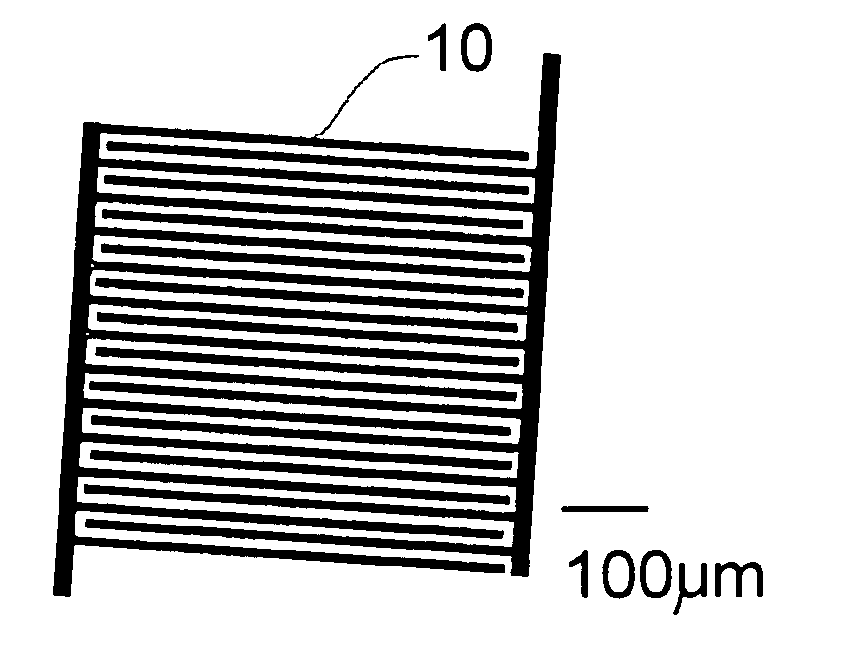
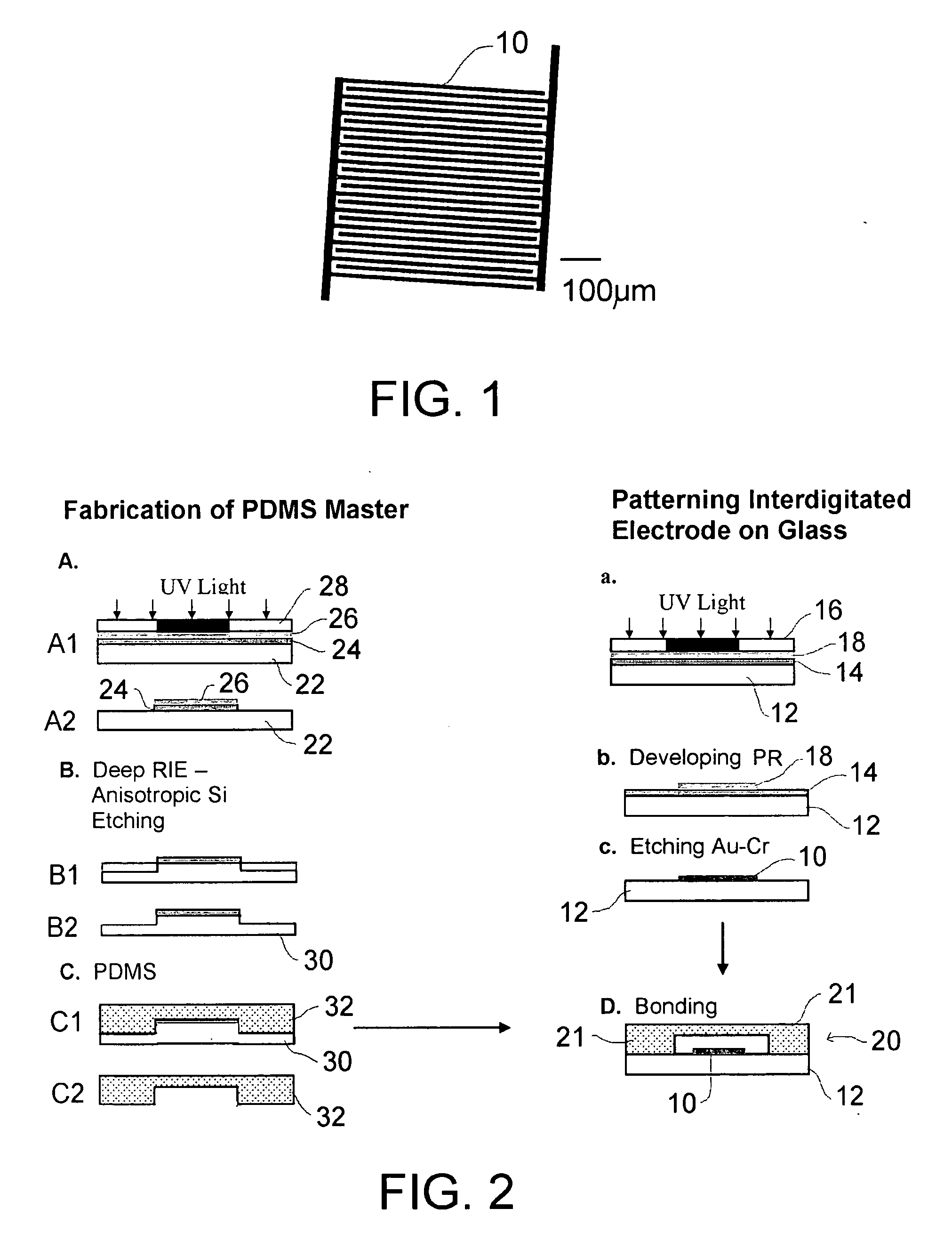
[0022] In this patent document, “comprising” is used in its inclusive sense and does not exclude other elements being present. In addition, the use of the indefinite article “a” before an element does not exclude others of that element being present. The electrodes referred to in this patent document are typically planar microelectrodes, where the term “micro” refers to features that are measured in microns, for example in the order of 10-200 microns.

[0023] Dielectric particles, such as intact biological cells, are electrically polarized when subjected to an alternating electric (A.C.) field. If this field is furthermore inhomogeneous, then the cells will experience a dielectrophoretic (DEP) force [5] that can act to convey them toward strong or weak field regions, depending on the dielectric polarization of the cell and that of the suspending medium [6,7,13].

[0024] The time averaged DEP force DEP> exerted by a non-uniform field of peak strength E acting on a homogenous spherical ...


PUM

PropertyMeasurementUnit
thicknessaaaaaaaaaa
thicknessaaaaaaaaaa
widthaaaaaaaaaa

Abstract

The design, development and fabrication of a DEP microfluidic assembly with an in-built interdigitated microelectrode array is presented. Continuous fractionation of microparticles in a PDMS microfluidic channel is described. Experimental verification of positive and negative DEP of yeast cells and polystyrene latex beads is demonstrated. A microfluidic device with DEP arranged electrodes in a channel has posts extending into the channel for controlling shaping of DEP fields.

Description

CROSS-REFERENCE TO RELATED APPLICATIONS [0001] This application claims the benefit under 35 USC 119(e) of provisional application 60 / 578,839 filed Jun. 14, 2004.BACKGROUND OF THE INVENTION [0002] Development of miniaturized total analysis systems (μTAS) is of increasing interest among the research community. Often referred to as ‘Laboratory-on-a-chip’, this technology offers new prospects for routine chemical analysis, drug testing, bioassay, health care delivery, and diagnostic devices including non-invasive early detection of cancers. For over a decade, the realization of miniaturized laboratory functions onto a microchip capable of performing rapid chemical / biochemical analyses using very small inventories of samples and reagents has been a challenging goal for many leading research groups world wide. Successful implementation of such μTAS devices of chips requires the integration of expertise from various disciplines. With the use of technologies from the microelectronics proces...

Claims


Application Information

Patent Timeline
Patent Type & Authority Applications(United States)
IPC IPC(8): B01L3/00B01L99/00B03C5/02G01N27/27H01S4/00
CPCB01L3/5027B03C5/026B81B2201/058Y10T29/49002
Inventor KANAGASABAPATHI, THIRUKUMARAN T.KALER, KARAN V.I.S.
Owner UNIV TECH INT
Why Eureka
Try Eureka