Method for fabricating magnetic field concentrators as liners around conductive wires in microelectronic devices
a magnetic field concentrator and microelectronic circuit technology, applied in solid-state devices, semiconductor devices, instruments, etc., can solve the problems of significant manufacturing complexity in physically realizing such magnetic liners in microelectronic circuitry, undesired material magnetic moment, and large current required to generate fields sufficient to switch the free layer
- Summary
- Abstract
- Description
- Claims
- Application Information
AI Technical Summary
Benefits of technology
Problems solved by technology
Method used
Image
Examples
first embodiment
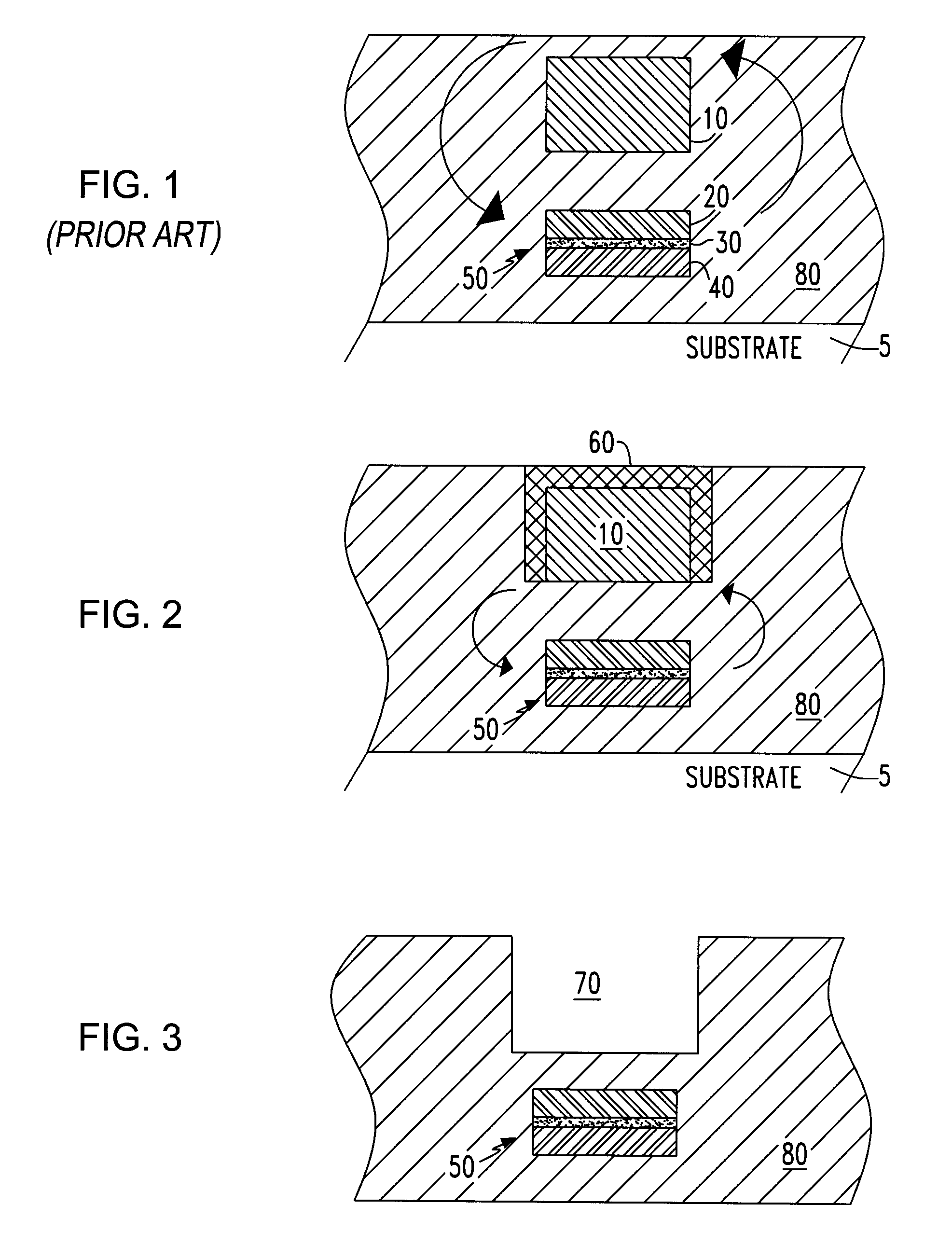
[0034] the second method (adding additional layers to deactivate undesired liner material) is diagramed in FIG. 6. FIG. 6 shows one version of the second of two preferred methods for deactivating or disabling the magnetic liner at the base of the trench: “pinning” the liner at the base of the trench with an antiferromagnet 90 deposited adjacent to the liner material. The term pinning is used routinely in the field to indicate that the magnetic moment of the material in question is strongly resistant to being changed by an applied magnetic field. Note that the antiferromagnet could also be deposited before the magnetic liner film 60. In either case, the antiferromagnet would be anisotropically deposited so that the bottom of the trench is more thickly covered than the sidewalls, and the sidewalls would have so little material that the antiferromagnetic pinning would be ineffective. The direction of the magnetic moment of the pinning material is preferably into or out of the page so a...
second embodiment
[0041] the second method (adding additional layers to deactivate undesired liner material) is illustrated in FIG. 7, showing a method for deactivating the magnetic liner at the base of the trench by effectively saturating the magnetization of the film at the base of the trench by creating an artificial antiferromagnet through the use of a coupling layer to promote synthetic antiferromagnetism with a second low reluctance liner layer.
[0042] In this situation, rather than using an antiferromagnet film to pin the undesired liner material, we disclose a method whereby an artificial, or synthetic antiferromagnet is created by depositing a coupling film 110 followed by a second magnetic film 120 that may be the same material as film 60. The coupling film material is chosen from the set of materials including Ru, Os, TaN, Re, Cr, CrMo, and similar, such that, at proper thickness, a strong antiferromagnetic exchange coupling is induced between the original magnetic liner film 60 and the sec...
PUM
 Abstract
Description
Claims
Application Information


