Low power and low timing jitter phase-lock loop and method

Inactive Publication Date: 2005-12-15
ROUND ROCK RES LLC
View PDF20 Cites 40 Cited by
  • Summary
  • Abstract
  • Description
  • Claims
  • Application Information

AI Technical Summary

Benefits of technology

[0014] A phase-lock loop and method is used to generate an output clock signal responsive to an input clock signal. The phase-lock loop includes a phase detector that generates a phase error signal indicative of a relationship between the phase of the input clock signal and the phase of the output clock signal. The phase-lock loop also includes a voltage controlled oscillator that generates a clock signal having a frequency corresponding the phase error signal. However, the clock signal from the voltage controlled oscillator is not used as the output clock signal. Instead, the clock signal from the voltage controlled oscillator is coupled to a frequency multiplier that generates the output clock signal with a frequency that is a multiple, such as an integer multiple, of the frequency of the clock signal generated by the voltage controlled oscillator. The vo

Problems solved by technology

However, the clock signal from the voltage controlle

Method used


Image

  • Low power and low timing jitter phase-lock loop and method
  • Low power and low timing jitter phase-lock loop and method
  • Low power and low timing jitter phase-lock loop and method

Examples


Embodiment Construction

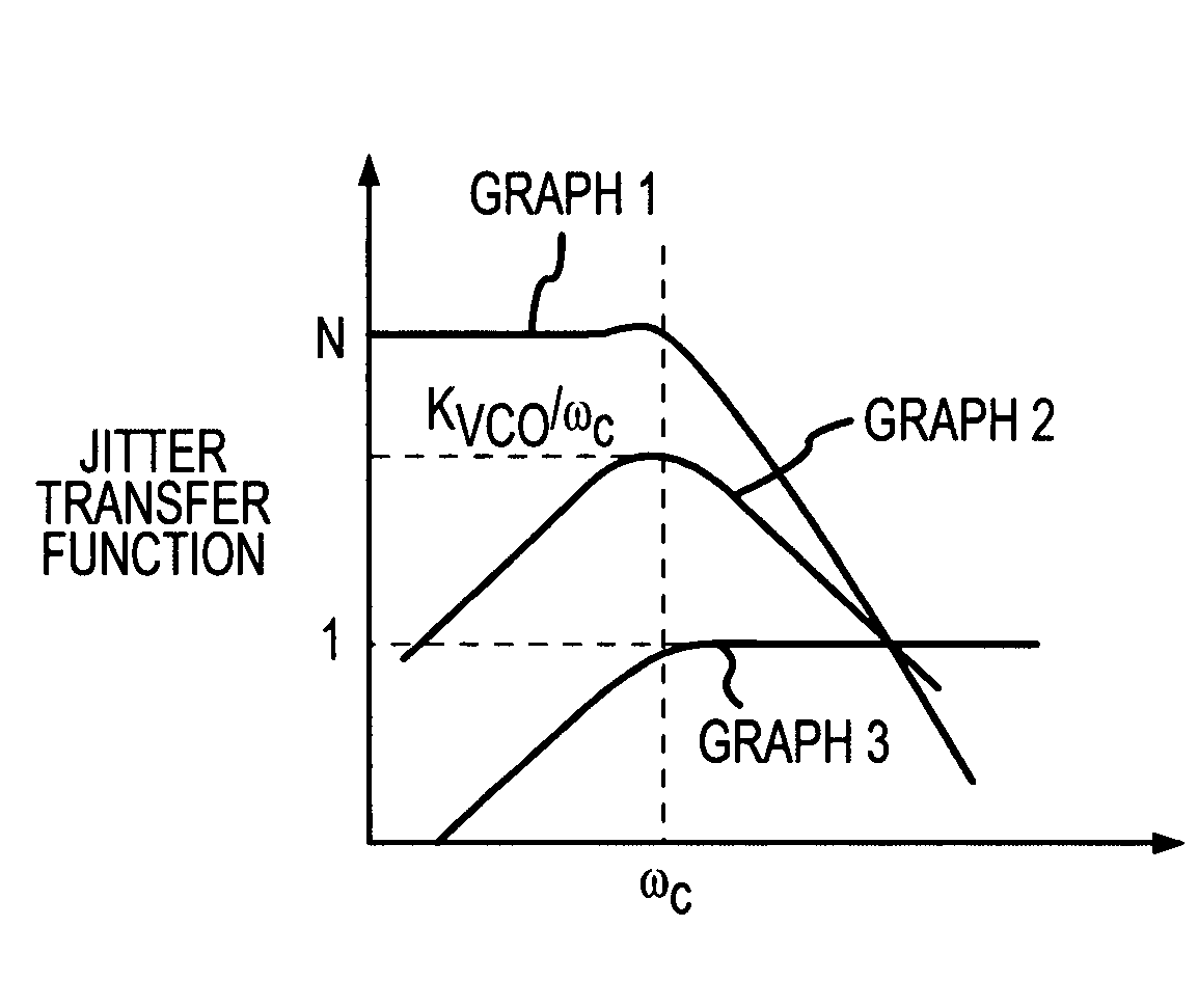
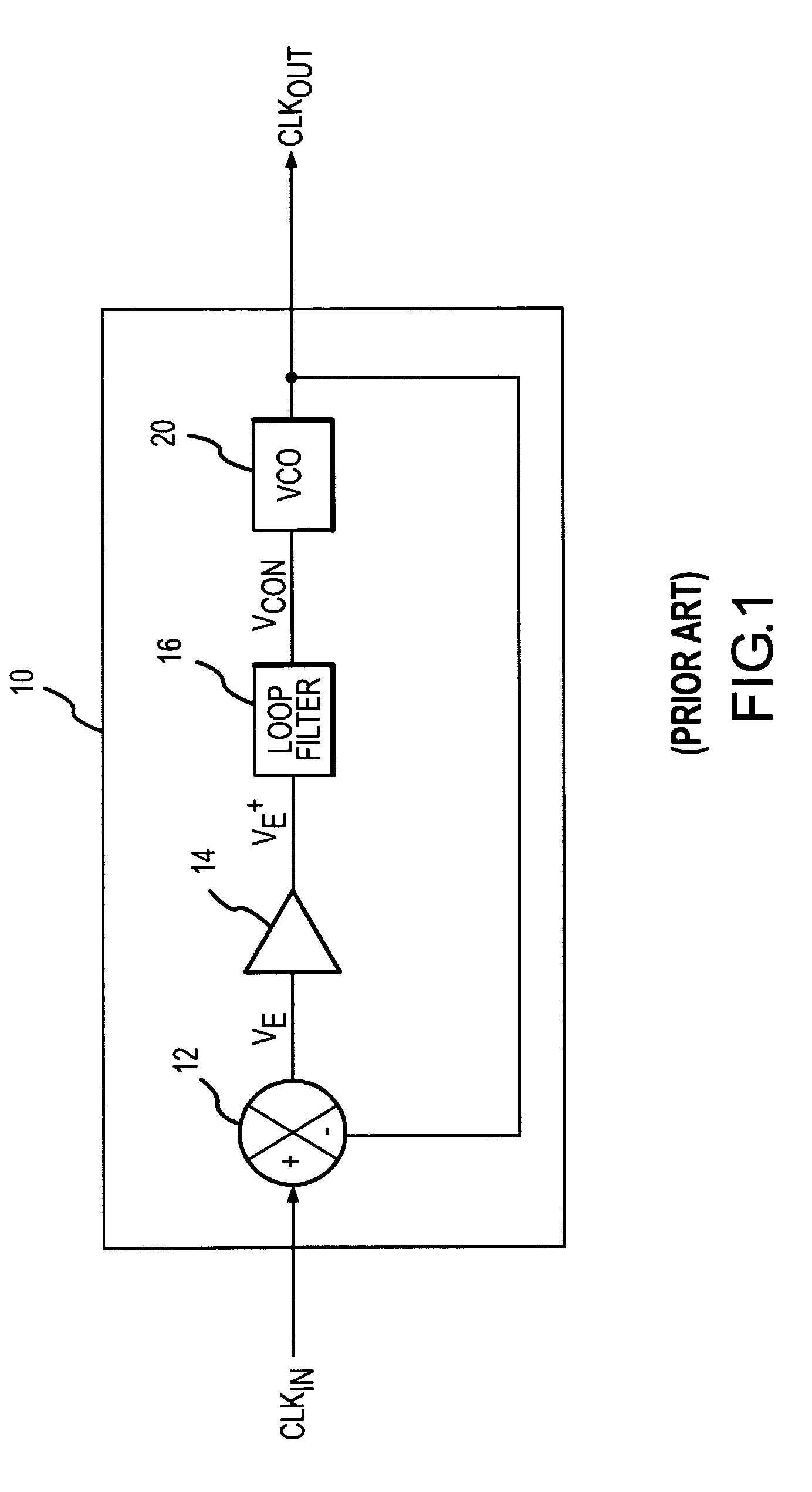
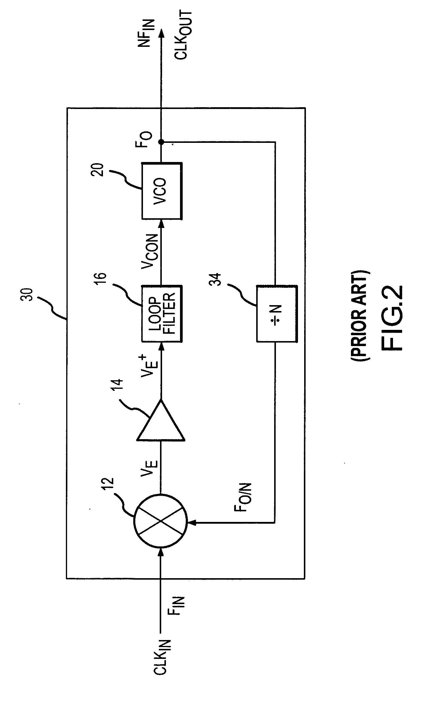
[0029] One embodiment of a phase-lock loop circuit 40 for generating an output clock signal CLKOUT from an input clock signal CLKIN in accordance with the present invention is shown in FIG. 5. The phase-lock loop 40 is similar in structure and operation to the phase-lock loop 10 of FIG. 1. Therefore, in the interest of brevity, identical components have been provided with the same reference numerals, and an explanation of their function and operation will not be repeated. The phase-lock loop 40 differs from the phase-lock loops 10, 30 by including a frequency multiplier 44 in the signal path from the VCO 20 to the phase detector 12. Also, the signal VOUT generated by the phase-lock loop 40 is taken at the output of the frequency multiplier 44 rather than at the output of the VCO 20 as in the phase-lock loop 30 of FIG. 2. The frequency multipler 44 is programmable to multiply the frequency of the signal at the output of the VCO 20 by any integer value N. Therefore, if the signal at t...


PUM


Abstract

A phase-lock loop generates an output clock signal from an input clock signal. The output clock signal is coupled through a clock tree and is fed back to a phase detector, which compares the phase of the output clock signal to the phase of the input clock signal. The output clock signal is generated by a voltage controlled oscillator having a control input coupled to receive an output from the phase detector, and a frequency multiplier coupled to the output of the voltage controlled oscillator. As a result, the CLKOUT signal generated by the frequency multiplier has a relatively high frequency while the voltage controlled oscillator, by operating at a relatively low frequency, uses relatively little power.

Description

TECHNICAL FIELD [0001] This invention relates to phase-lock loops for generating one or more clock signals from an input clock signal. BACKGROUND OF THE INVENTION [0002] Periodic digital signals are commonly used in a variety of electronic devices. Probably the most common of periodic digital signals are clock signals that are typically used to establish the timing of a digital signal or the timing at which an operation is performed on a digital signal. For example, data signals are typically coupled to and from memory devices, such as synchronous dynamic random access memory (“SDRAM”) devices, in synchronism with a clock or data strobe signal. [0003] As the speed of memory devices and other devices continue to increase, the “eye” or period in which a digital signal, such as a data signal, is valid becomes smaller and smaller, thus making the timing of a strobe signal or other clock signal used to capture the digital signal even more critical. In particular, as the size of the eye b...

Claims


Application Information

Patent Timeline
IPC IPC(8): G06F1/04H03L7/00H03L7/099
CPCG06F1/04G11C7/02G11C7/1006G11C7/1018G11C7/1051G11C7/1078G11C7/22G11C7/222G11C8/18G11C11/406G11C11/4076G11C11/4093H03L7/0891H03L7/0995H03L7/16H03L2207/10H03L7/00
Inventor CHOI, DONG MYUNG
Owner ROUND ROCK RES LLC
Why Eureka
Try Eureka