Fabrication method of wafer level chip scale packages

Active Publication Date: 2005-12-15
SAMSUNG ELECTRONICS CO LTD
View PDF17 Cites 59 Cited by
  • Summary
  • Abstract
  • Description
  • Claims
  • Application Information

AI Technical Summary

Benefits of technology

[0011] Exemplary, non-limiting embodiments of the present invention may provide a fabrication method of a wafer level chip scale package (WLCSP) for a p

Problems solved by technology

For example, the wafer, which may be fabricated from silicon, may be inherently brittle.
Thus, a relatively thin wafer (which may result after grinding) may not exhibit good reliability during fabrication and handling.
Further, it may be difficult to form the wiring plug in the hole penetrating completely through the wafer.
Moreover, the formation of the metal bump may require a complicated, lengthy and expensive process since the metal bump may be typically formed by photolithogr

Method used


Image

  • Fabrication method of wafer level chip scale packages
  • Fabrication method of wafer level chip scale packages
  • Fabrication method of wafer level chip scale packages

Examples


Example

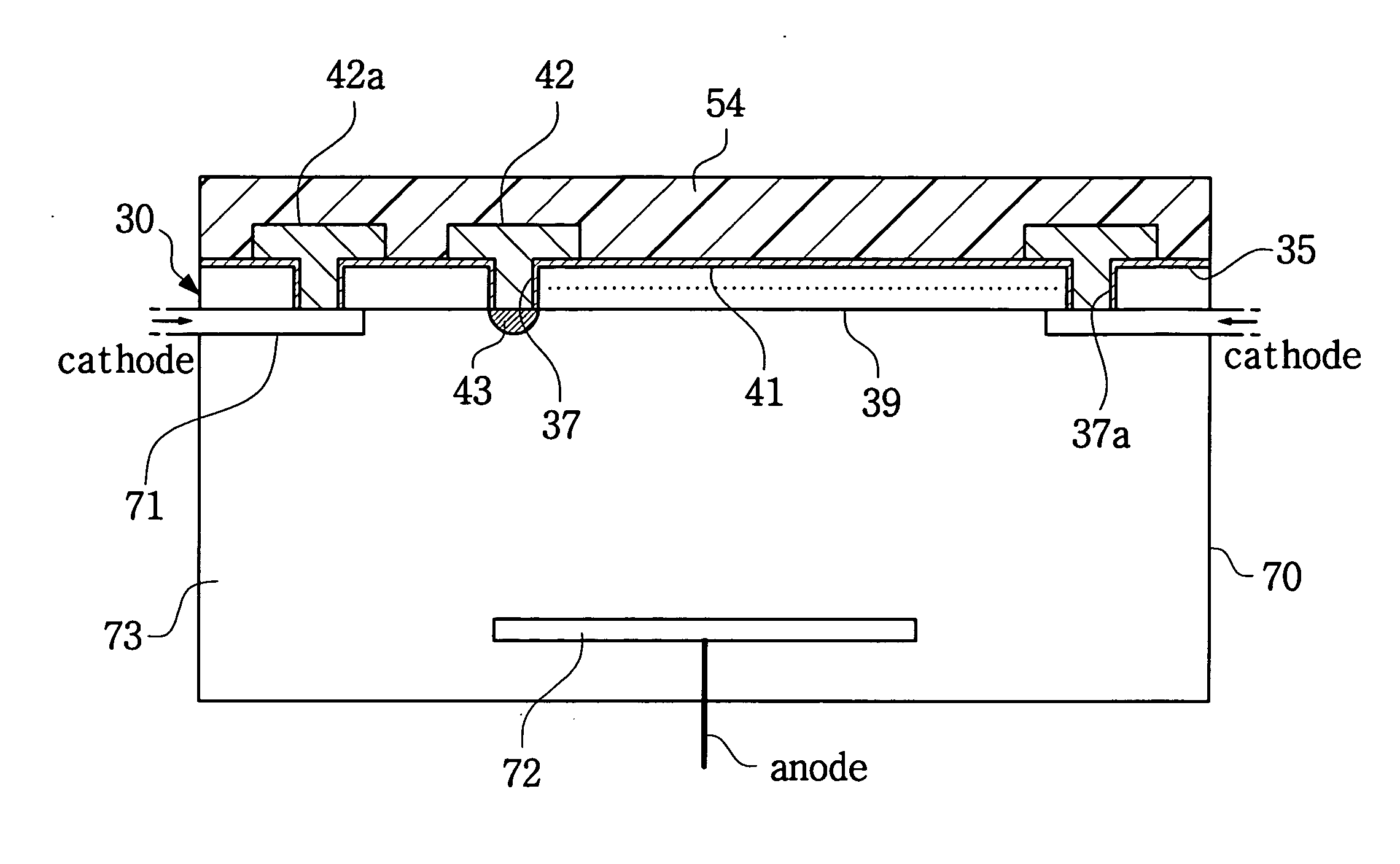
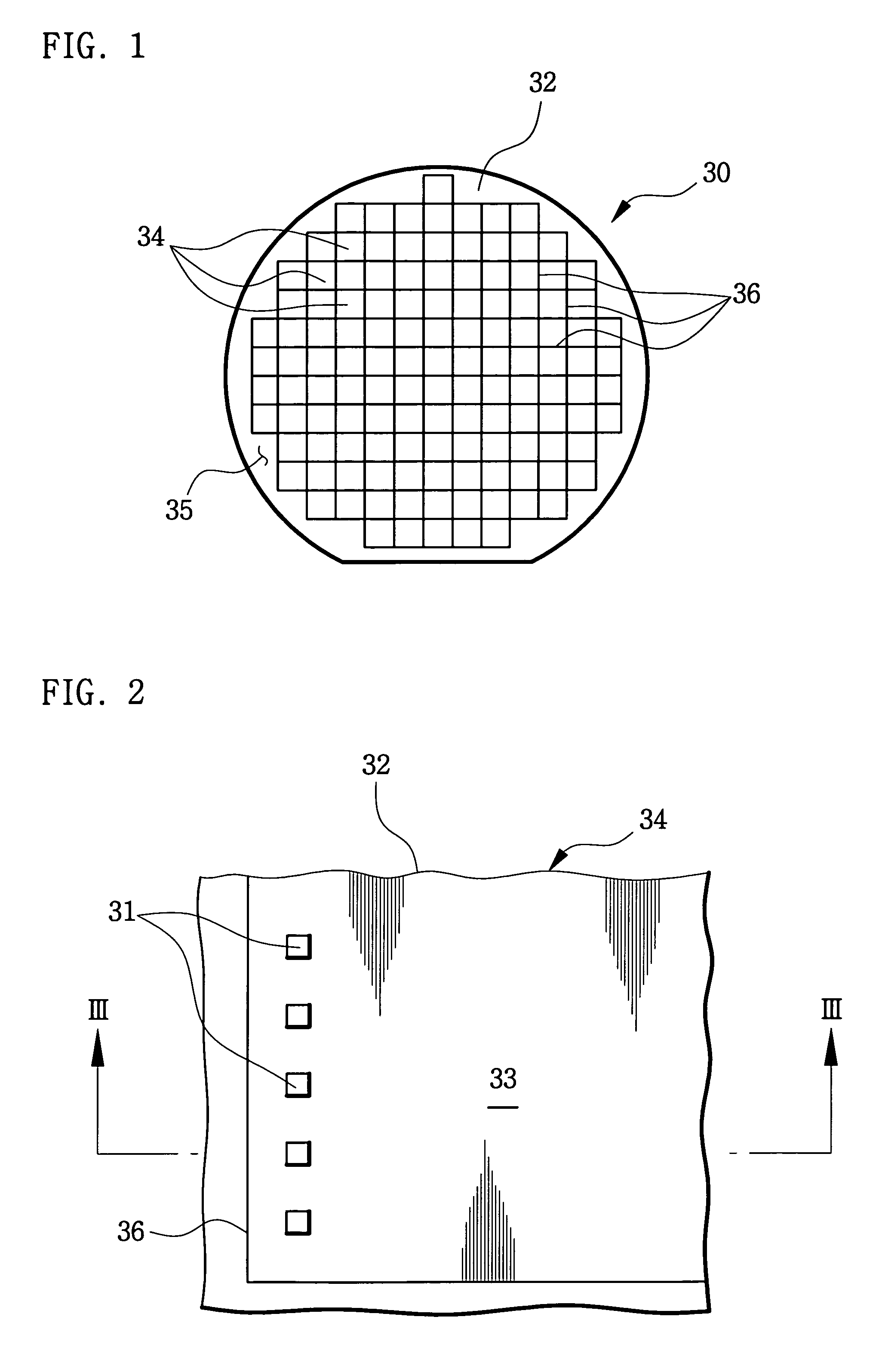
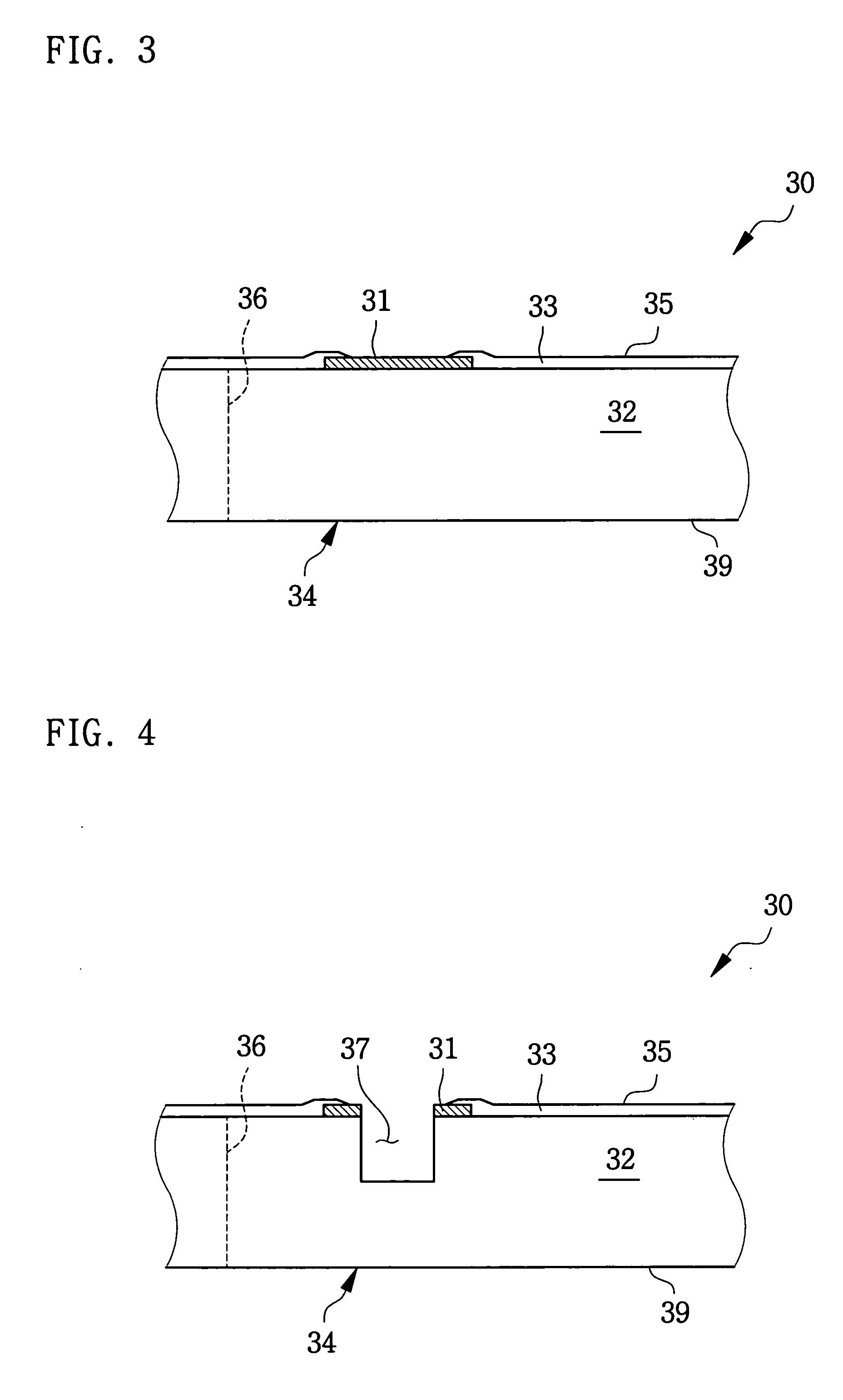
[0036] Exemplary, non-limiting embodiments of the present invention will now be described more fully with reference to the accompanying drawings. This invention may, however, be embodied in many different forms and should not be construed as limited to the exemplary embodiments. Rather, the disclosed embodiments are provided so that this disclosure will be thorough and complete, and will fully convey the scope of the invention to those skilled in the art. The principles and feature of this invention may be employed in varied and numerous embodiments without departing from the scope of the invention.

[0037] In this disclosure, well-known structures and processes may not described or illustrated in detail to avoid obscuring the present invention. Furthermore, the figures are not drawn to scale. Rather, for simplicity and clarity of illustration, the dimensions of some of the elements may be exaggerated relative to other elements. A layer may be considered as being formed (or otherwise...


PUM

PropertyMeasurementUnit
aaaaaaaaaa

Abstract

A method of fabricating wafer level chip scale packages may involve forming a hole to penetrate through a chip pad of an IC chip. A base metal layer may be formed on a first face of a wafer to cover inner surfaces of the hole. An electrode metal layer may fill the hole and rise over the chip pad. A second face of the wafer may be grinded such that the electrode metal layer in the hole may be exposed through the second face. By electroplating, a plated bump may be formed on the electrode metal layer exposed through the second face. The base metal layer may be selectively removed to isolate adjacent electrode metal layers. The wafer may be sawed along scribe lanes to separate individual packages from the wafer.

Description

CROSS REFERENCE TO RELATED APPLICATIONS [0001] This U.S. non-provisional application claims priority under 35 U.S.C. §119 from Korean Patent Application No. 2004-44050, which was filed in the Korean Intellectual Property Office on Jun. 15, 2004, the contents of which are incorporated by reference herein in its entirety. BACKGROUND OF THE INVENTION [0002] 1. Field of the Invention [0003] The present invention relates generally to electronic packaging technology and, more particularly, to a fabrication method of wafer level chip scale packages available for a three-dimensional package stack. [0004] 2. Description of the Related Art [0005] As in other sectors of the semiconductor industry, the electronic packaging industry may be driven by a demand for packages that may be smaller, faster, cheaper, more reliable, and more multi-functional, for example. A chip scale package (CSP), which may be referred to as a chip size package, has been developed to satisfy the industry's growing deman...

Claims


Application Information

Patent Timeline
IPC IPC(8): C25D5/02H01L23/28C25D7/12H01L21/288H01L21/48H01L21/60H01L21/768H01L23/31H01L23/48
CPCC25D5/02H01L2224/0401H01L21/2885H01L21/76898H01L23/3114H01L23/481H01L24/03H01L24/05H01L24/11H01L2224/05599H01L2224/05639H01L2224/05644H01L2224/05647H01L2224/13009H01L2224/13025H01L2224/13099H01L2224/16H01L2924/01004H01L2924/01006H01L2924/01013H01L2924/01014H01L2924/01022H01L2924/01028H01L2924/01029H01L2924/01046H01L2924/01047H01L2924/01075H01L2924/01078H01L2924/01079H01L2924/014H01L2924/05042H01L2924/14H01L2924/01024H01L2924/01033H01L2924/00014C25D7/12H01L2224/05554H01L2224/02166H01L2924/12042C25D5/022C25D7/123H01L2924/00H01L23/28
Inventor KIM, SOON-BUMKIM, UNG-KWANGMA, KEUM-HEESONG, YOUNG-HEESIM, SUNG-MINOH, SE-YONGLEE, KANG-WOOKJEONG, SE-YOUNG
Owner SAMSUNG ELECTRONICS CO LTD
Why Eureka
Try Eureka