Sensors with Gradient Nanostructures and Associated Method of Use
a nanostructure, nano-structure technology, applied in measurement devices, instruments, scientific instruments, etc., can solve the problem that colorimetric sensors cannot provide highly accurate, etc., and achieve the effect of high accuracy, time-saving and cost-effectiv
- Summary
- Abstract
- Description
- Claims
- Application Information
AI Technical Summary
Benefits of technology
Problems solved by technology
Method used
Image
Examples
example 1
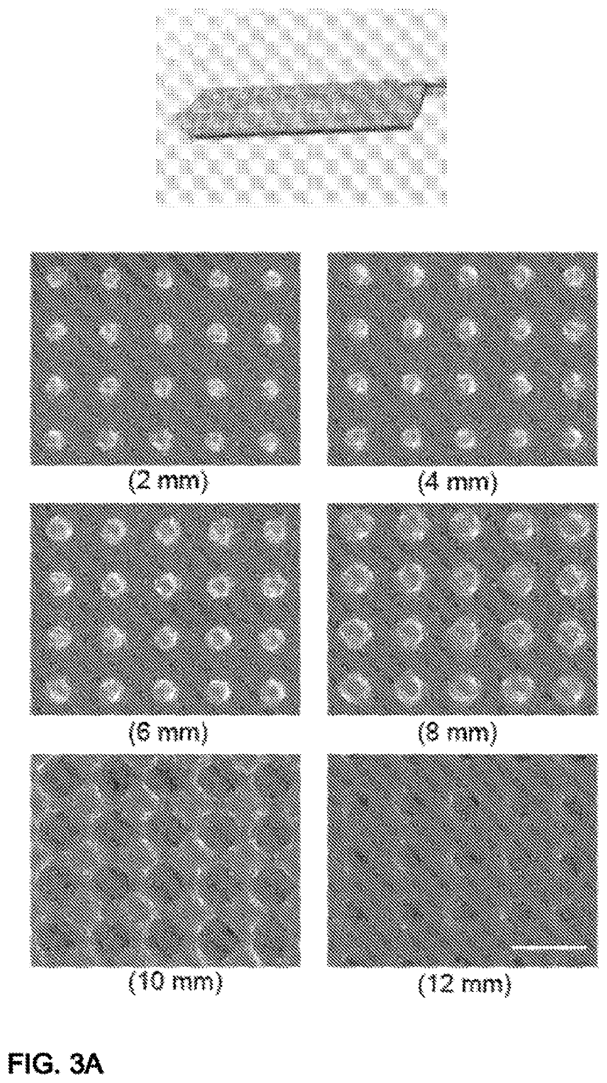
[0030]An embodiment of the present invention was fabricated as seen in FIGS. 3A-B, In the sensor embodiment of FIGS. 3A-B, a sensor with pillar-hole structures covered by gold disks and nano-hole plane was fabricated using the above stated fabrication procedure with interference lithography being used to pattern the resist.
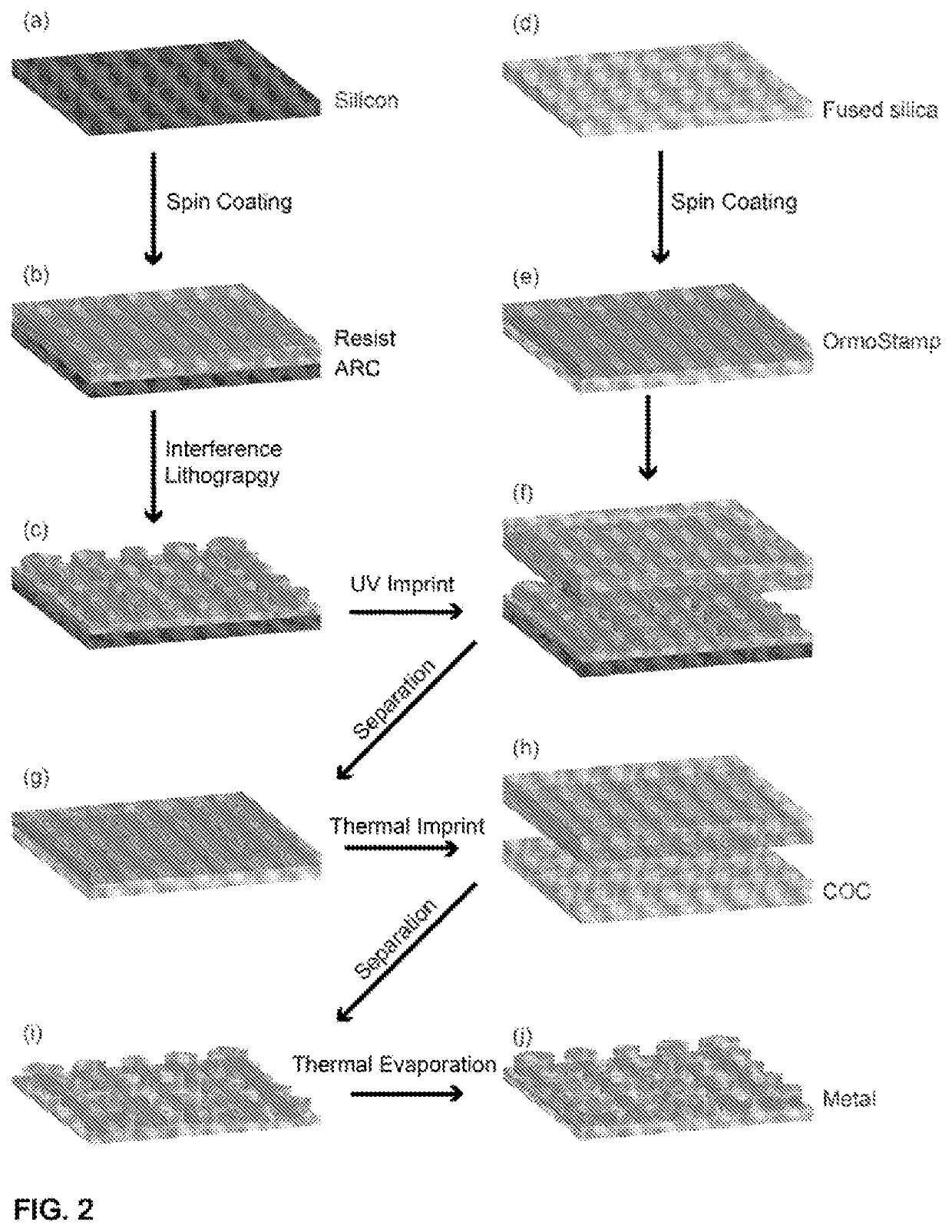
[0031]FIG. 3A shows the gradient color rings displayed by gradient nanostructures on a silicon substrate. SEM characterizations show the nano pillars and holes at different radial distances in the resist. The nanostructures have a period of 370 nm Then the gradient pattern was transferred to a fused silica wafer by UV imprint lithography to create a thermal imprint template. Then, a thermoplastic film such as a cyclic olefin copolymer (“COC”) film was placed on the fused silica template with a gradient pattern, heated, pressed and separated. Finally, an 80 nm gold layer was deposited on the COC film by thermal evaporation. As a result, a sensor with pillar-hole st...
example 2
[0033]A gradient-pattern plasmonic sensor according to an embodiment of the present invention can be used in a spectrometer-free way. A schematic of an approach for using the gradient-pattern plasmonic sensor according to an embodiment of the present invention can be seen in FIG. 4. The setup used for liquid refractive index measurement using a sensor 10 with pillar-hole structures covered by gold disks and nano-hole planes according to an embodiment of the present invention includes: (i) a white illumination light source 40, illuminating the sensor 10 from the back side; (ii) the sensor is covered with refractive index liquid 42; and (iii) a camera 44 taking pictures from the front side. The camera may be a cellphone camera or a CMOS or a CCD camera. The liquid 42 can be any one of a number of functional materials, e.g., palladium, hydrogel, an antibody, protein, gas molecules, ions in water, antigen and DNA.
[0034]In one arrangement an iPhone was used with a white background screen...
PUM
| Property | Measurement | Unit |
|---|---|---|
| height | aaaaa | aaaaa |
| height | aaaaa | aaaaa |
| thickness | aaaaa | aaaaa |
Abstract
Description
Claims
Application Information


