

Matrix optical process correction
a technology of matrix optical process and layout verification, applied in the direction of photomechanical treatment originals, photomechanical instruments, photomechanical apparatus, etc., can solve the problems of circuit elements to be created on a wafer, and affecting the appearance of the obj
- Summary
- Abstract
- Description
- Claims
- Application Information
AI Technical Summary
Benefits of technology
Problems solved by technology
Method used
Image

Examples
Embodiment Construction
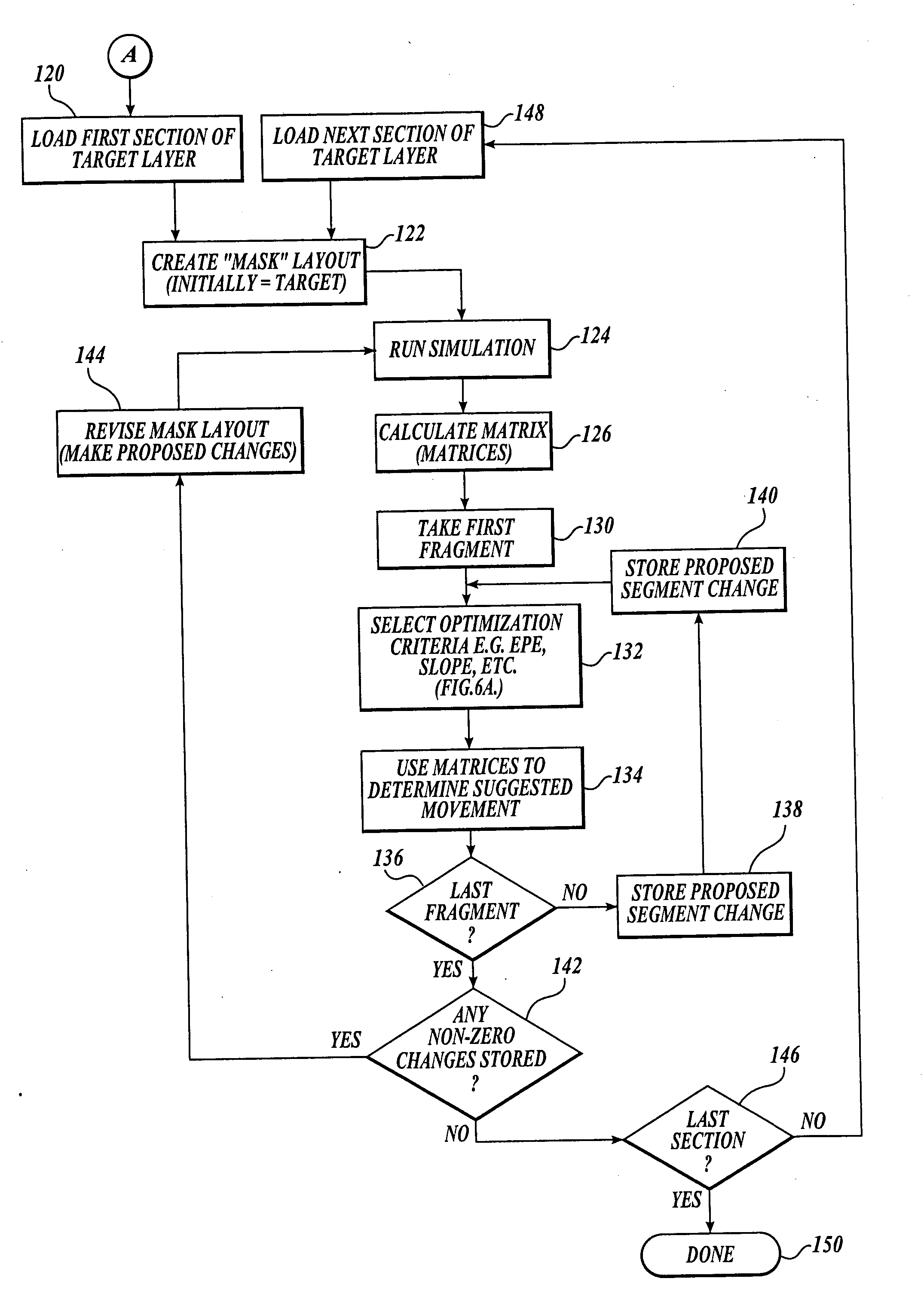
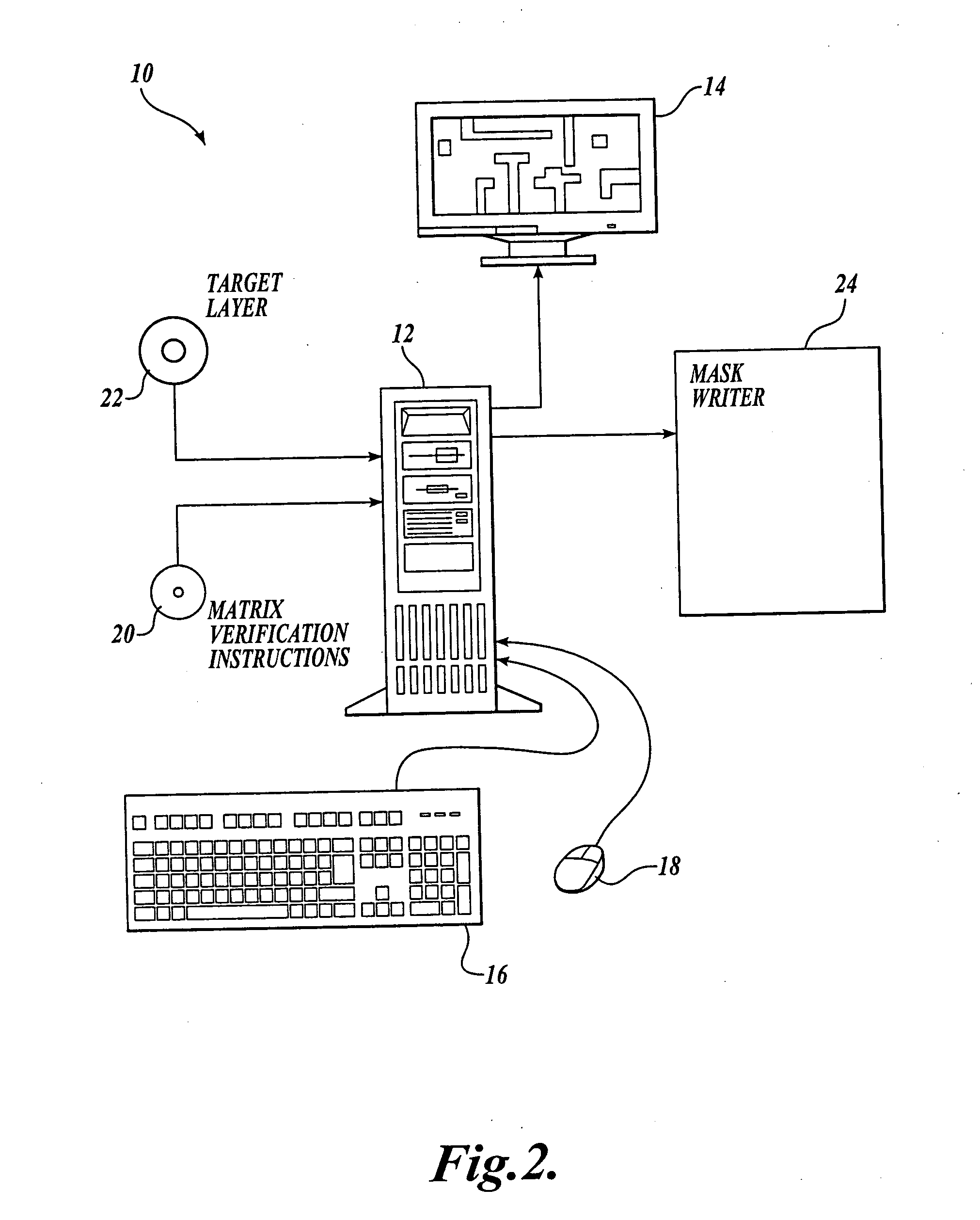
[0021]FIG. 2 illustrates one embodiment of a computer system that is used to perform a matrix-based verification technique such optical process correction (OPC) in accordance with the present invention. The computer system 10 includes a stand-alone or networked processor 12 having a visual display 14 and data input mechanism such as a keyboard 16 and mouse 18. Instructions used by the processor 12 to implement the matrix-based verification technique of the present invention are received on a computer readable media such as a CD-ROM or DVD 20 or can be received as a communication signal from a remote computer over a wired or wireless data link. As will be described in further detail below, the processor 12 receives a target layer description that defines a number of circuit elements to be created on a semiconductor wafer. The target layer description is received on a computer readable media 22 or can be received from a remote computer over a wired or wireless data communication link....
PUM
| Property | Measurement | Unit |
|---|---|---|
| optical radius | aaaaa | aaaaa |
| photosensitive | aaaaa | aaaaa |
| size | aaaaa | aaaaa |
Abstract
Description
Claims
Application Information