Strained tri-channel layer for semiconductor-based electronic devices

Active Publication Date: 2005-12-22
MASSACHUSETTS INST OF TECH
View PDF19 Cites 42 Cited by
  • Summary
  • Abstract
  • Description
  • Claims
  • Application Information

AI Technical Summary

Benefits of technology

[0010] The invention arises, in part, from the realization that a significant portion of the decline in hole mobility in a Si1-xGex channel layer can arise from a substantial loss of Ge concentration of the channel layer during device processing; a loss in Ge concentration can be substantially reduced by placing a diffusion barrier layer beneath the channel layer. The invention further arises from the realization that a strained silicon layer, disposed below and in contact with a Si1-xGex, channel layer, can effectively impede diffusion of Ge from the Si1-xGex channel layer. A substantially pure Si layer provides a particularly effective barrier layer because of the relatively slow diffu

Problems solved by technology

Above a certain critical thickness of the deposited layer, however, misfit dislocations typically form at the layer interface.
Unfortunately, Si1-xGex-based substrates can increase the comp

Method used


Image

  • Strained tri-channel layer for semiconductor-based electronic devices
  • Strained tri-channel layer for semiconductor-based electronic devices
  • Strained tri-channel layer for semiconductor-based electronic devices

Examples


Embodiment Construction

[0025] This invention is not limited in its application to the details of construction and the arrangement of components set forth in the following description or illustrated in the drawings. The invention is capable of other embodiments and of being practiced or of being carried out in various ways. Also, the phraseology and terminology used herein is for the purpose of description and should not be regarded as limiting. The use of “including,”“comprising,” or “having,”“containing,”, “involving,” and variations thereof herein, is meant to encompass the items listed thereafter and equivalents thereof as well as additional items.

[0026] The present invention will now be described by way of specific, non-limiting, examples. It should be understood that the invention applies to substrates, devices, and fabrication methods beyond those discussed here. Specific structures, devices, and fabrication steps are meant for illustrative purposes only, and are non-limiting.

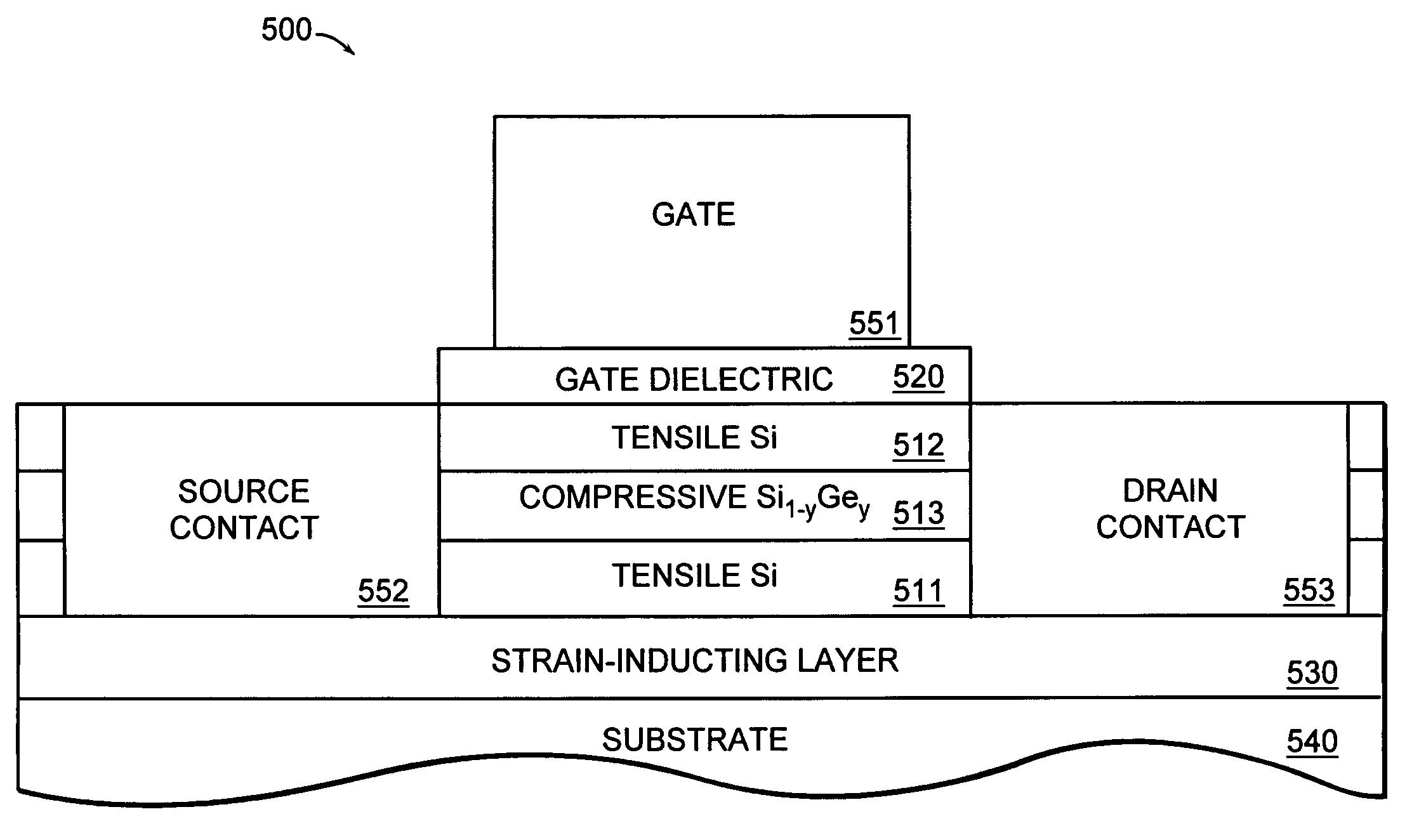
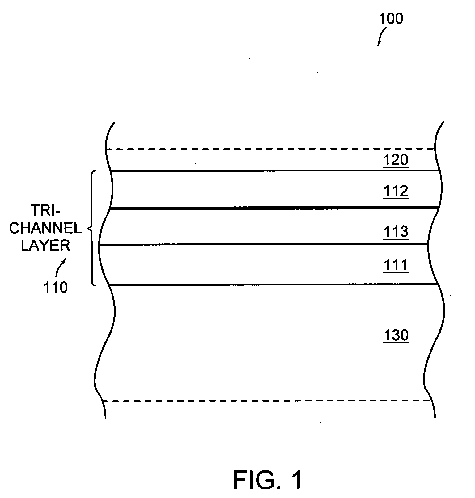
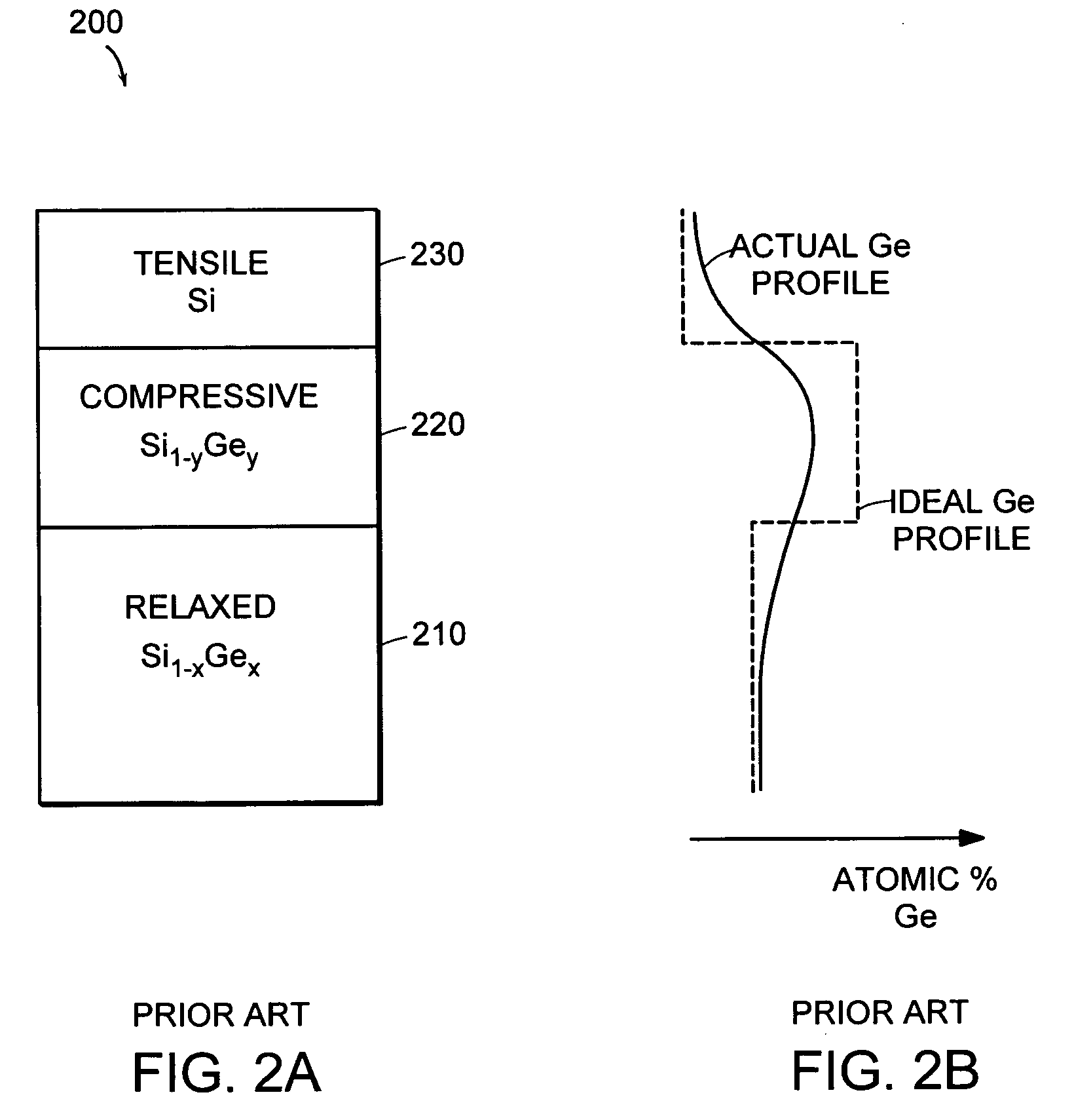
[0027] The invention ...


PUM


Abstract

A semiconductor-based structure includes a substrate layer, a compressively strained semiconductor layer adjacent to the substrate layer to provide a channel for a component, and a tensilely strained semiconductor layer disposed between the substrate layer and the compressively strained semiconductor layer. A method for making an electronic device includes providing, on a strain-inducing substrate, a first tensilely strained layer, forming a compressively strained layer on the first tensilely strained layer, and forming a second tensilely strained layer on the compressively strained layer. The first and second tensilely strained layers can be formed of silicon, and the compressively strained layer can be formed of silicon and germanium.

Description

BACKGROUND OF INVENTION [0001] 1. Field of Invention [0002] The invention relates to semiconductor-based electronic devices, and, more particularly, to the structure and fabrication of semiconductor-based substrates and electronic devices that include strained semiconductor layers. [0003] 2. Discussion of Related Art [0004] Some advanced semiconductor-based devices include a semiconductor layer that is strained by application of a stress to provide improved performance of the devices. For example, metal-oxide-semiconductor (MOS) transistors having a channel formed in strained silicon or strained Si1-yGey formed on unstrained, or relaxed, Si1-xGex, can exhibit improved carrier mobility in comparison to traditional p-type MOS (PMOS) and n-type MOS (NMOS) transistors. Strained-layer MOS transistors can be formed on “virtual substrates,” which include a strained layer to provide compatibility with traditional silicon-based fabrication equipment and methods that were designed for use wit...

Claims


Application Information

Patent Timeline
IPC IPC(8): H01L21/3205H01L21/8238H01L29/06H01L29/10H01L29/49H01L31/0336
CPCH01L21/823807H01L29/1054H01L29/4966H01L29/4925H01L29/495H01L29/4916
Inventor GUPTA, SAURABHLEE, MINJOO LARRYFITZGERALD, EUGENE A.
Owner MASSACHUSETTS INST OF TECH
Why Eureka
Try Eureka