Complementary metal oxide semiconductor (CMOS) transistors having three-dimensional channel regions and methods of forming same

a metal oxide semiconductor and channel region technology, applied in the direction of transportation and packaging, transportation items, items transportation vehicles, etc., can solve the problems of parasitic short-channel effects of metal oxide semiconductor (mos) transistors having reduced channel lengths, higher inversion-layer channel resistance, and complications, etc., to achieve unique and even optimal characteristics, reduce p-channel mobility, and wide channel width

Active Publication Date: 2005-09-29
SAMSUNG ELECTRONICS CO LTD
View PDF8 Cites 103 Cited by
  • Summary
  • Abstract
  • Description
  • Claims
  • Application Information

AI Technical Summary

Benefits of technology

[0005] Embodiments of the invention include an integrated circuit device contains a semiconductor substrate and a NMOS transistor having a first fin-shaped active region that extends in the semiconductor substrate. The first fin-shaped active region has a first three-dimensional channel region therein with a first height. A PMOS transistor is also provided. The PMOS transistor has a second three-dimensional fin-shaped active region that extends in the semiconductor substrate. The second fin-shaped active region has a second channel region therein with a second height unequal to the first height. These unequal heights of the channel regions enable the NMOS and PMOS transistors to have unique and even optimum characteristics. For example, a greater height of the channel region in the PMOS transistor relative to a height of the channel region in the NMOS transistor translates to a wider channel width. This wider channel width can compensate for the lower P-channel mobility of the PMOS transistor (e.g., lower hole mobility in an inversion-layer channel during forward on-state conduction) relative to N-channel mobility in the NMOS transistor.

Problems solved by technology

Metal oxide semiconductor (MOS) transistors having reduced channel lengths may suffer from parasitic short-channel effects.
Unfortunately, this higher doping concentration may result in a higher inversion-layer channel resistance when the transistor is disposed in a forward on-state mode of operation.
Notwithstanding these methods, complications may arise when forming complementary metal oxide semiconductor (CMOS) transistors in a semiconductor substrate.
These complications may relate to the inability to obtain optimum device characteristics for both NMOS and PMOS transistors because of the fact that electron and hole mobilities in these transistors are different.
However, these unique processing conditions may be difficult to apply to conventional CMOS methods of forming channel regions having three-dimensional shapes (e.g., fin-shaped channel regions).

Method used


Image

  • Complementary metal oxide semiconductor (CMOS) transistors having three-dimensional channel regions and methods of forming same
  • Complementary metal oxide semiconductor (CMOS) transistors having three-dimensional channel regions and methods of forming same
  • Complementary metal oxide semiconductor (CMOS) transistors having three-dimensional channel regions and methods of forming same

Examples


Embodiment Construction

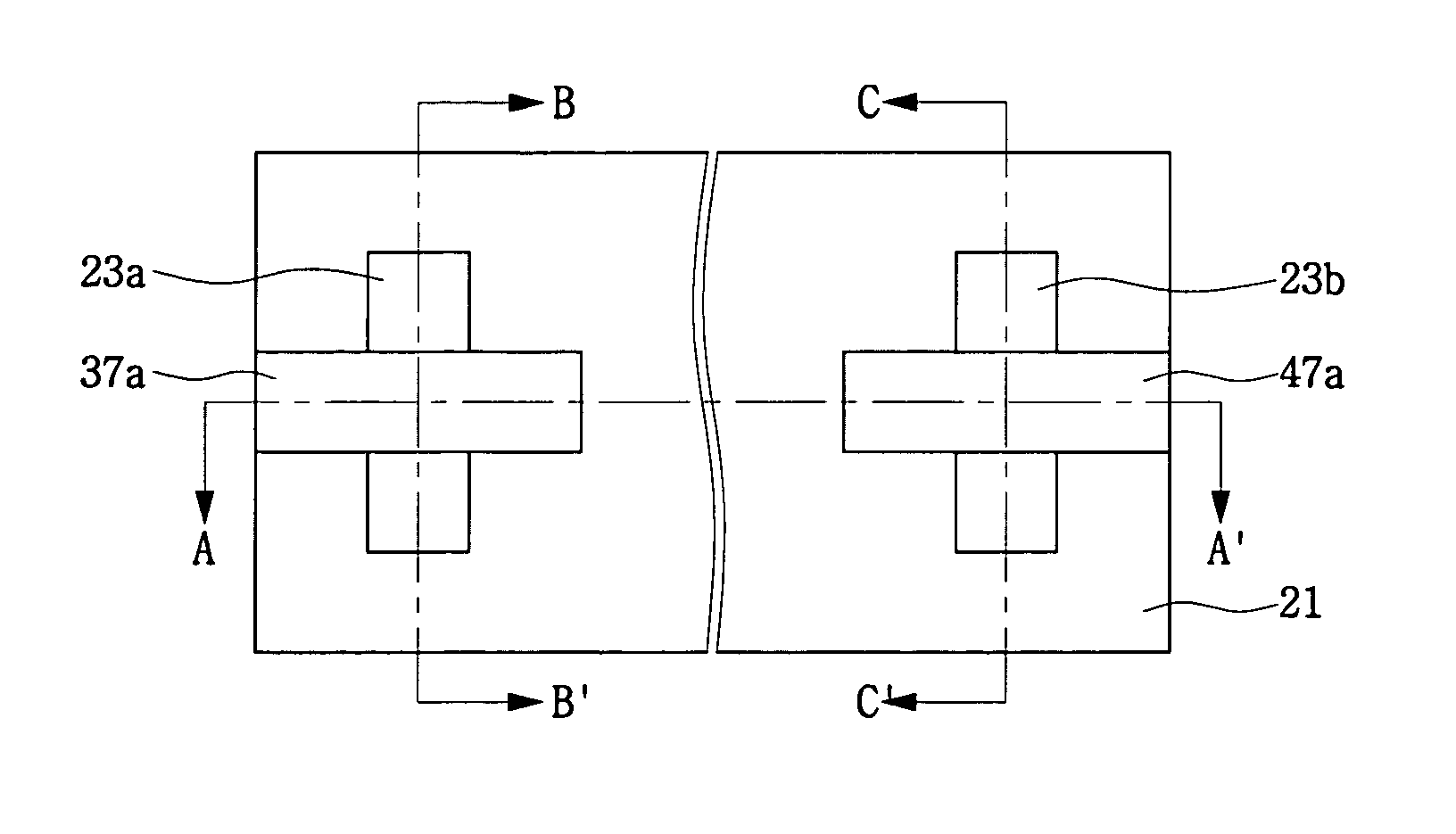
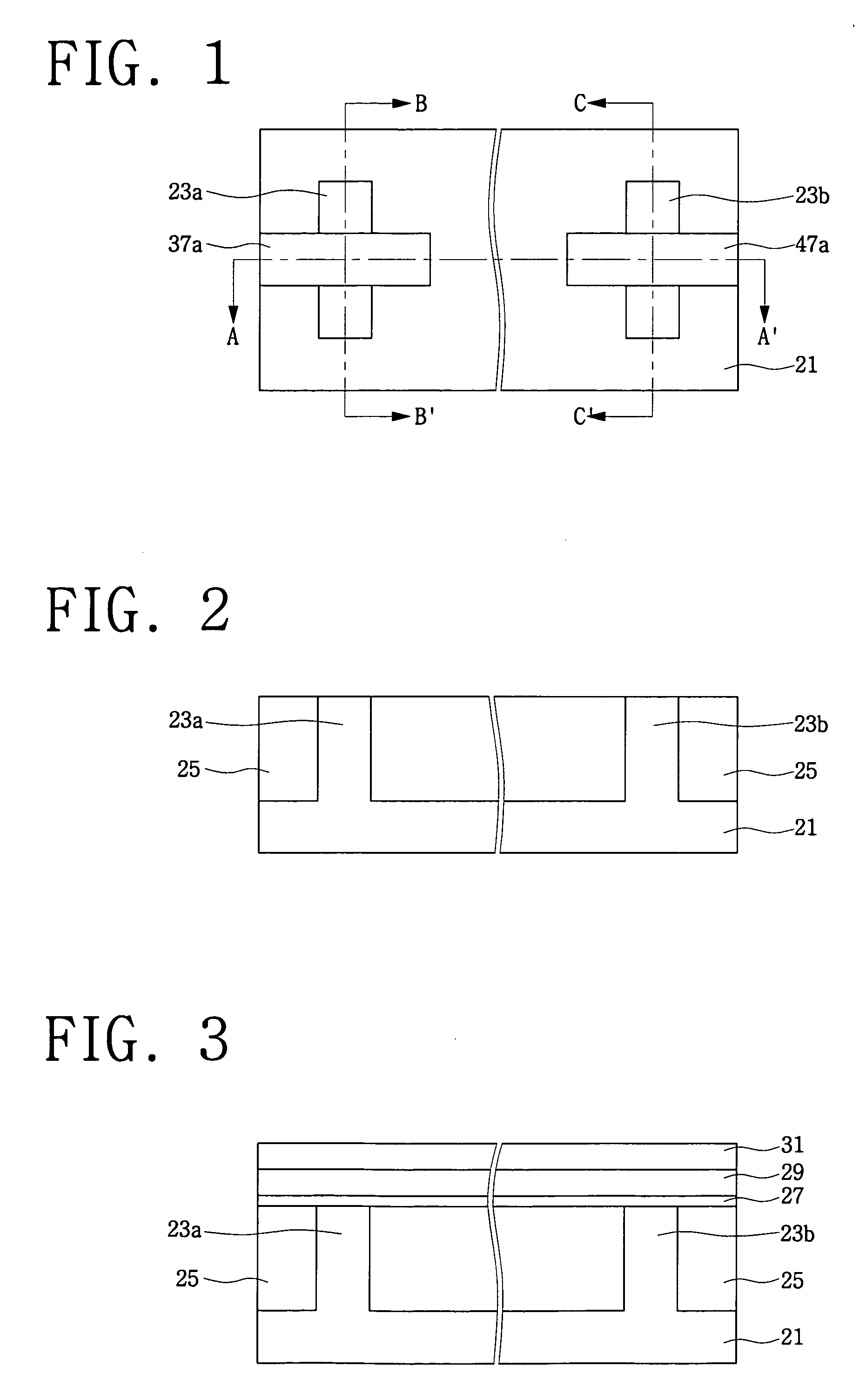
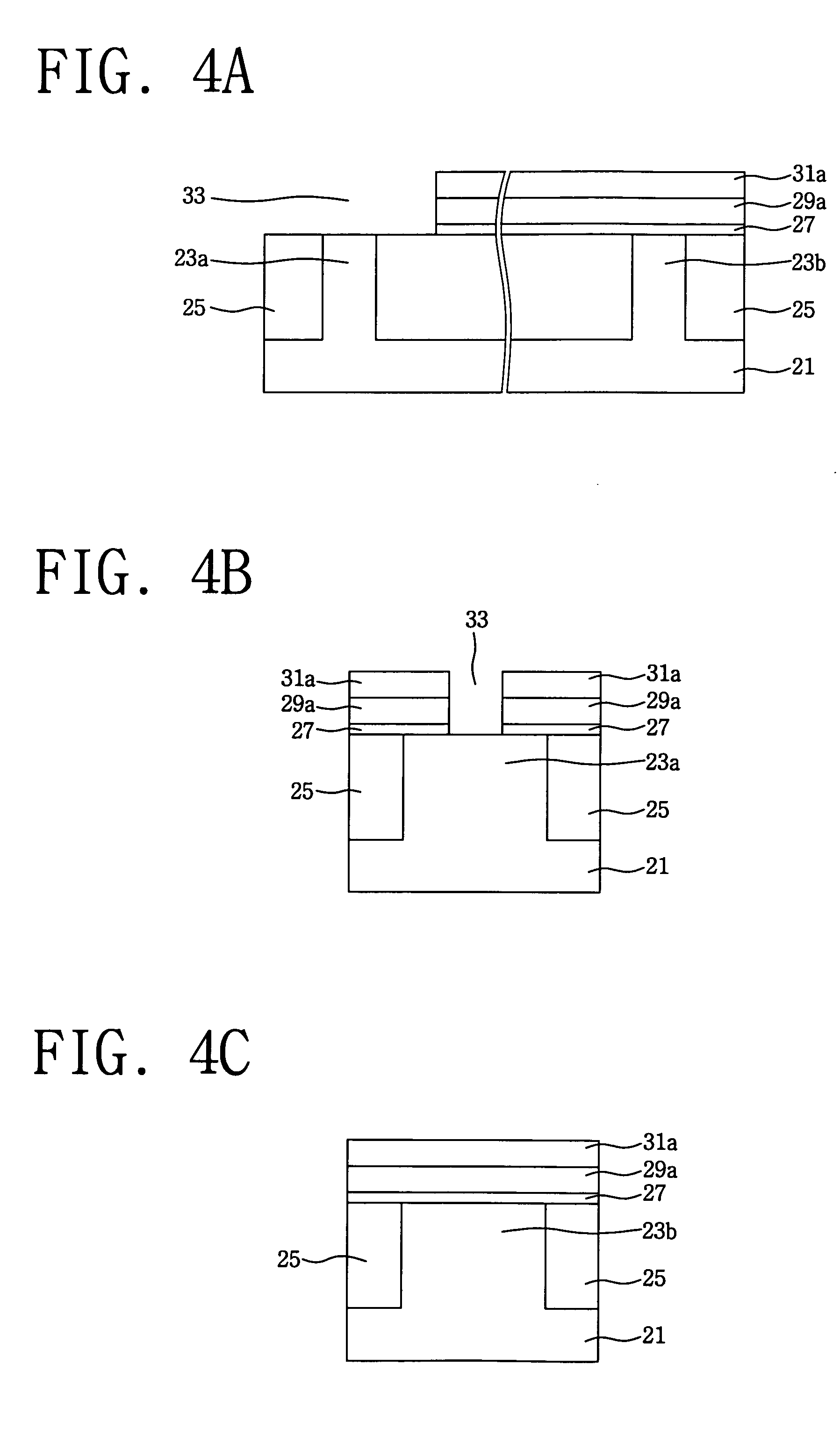
[0014] The present invention now will be described more fully herein with reference to the accompanying drawings, in which preferred embodiments of the invention are shown. This invention may, however, be embodied in many different forms and should not be construed as being limited to the embodiments set forth herein; rather, these embodiments are provided so that this disclosure will be thorough and complete, and will fully convey the scope of the invention to those skilled in the art. In the drawings, the thickness of layers and regions are exaggerated for clarity of description. It will also be understood that when a layer is referred to as being “on” another layer or substrate, it can be directly on the other layer or substrate, or intervening layers may also be present. Moreover, the terms “first conductivity type” and “second conductivity type” refer to opposite conductivity types such as N or P-type, however, each embodiment described and illustrated herein includes its compl...


PUM


Abstract

An integrated circuit device containing complementary metal oxide semiconductor transistors includes a semiconductor substrate and an NMOS transistor having a first fin-shaped active region that extends in the semiconductor substrate. The first fin-shaped active region has a first channel region therein with a first height. A PMOS transistor is also provided. The PMOS transistor has a second fin-shaped active region that extends in the semiconductor substrate. This second fin-shaped active region has a second channel region therein with a second height unequal to the first height.

Description

REFERENCE TO PRIORITY APPLICATION [0001] This application claims priority to Korean Application Ser. No. 2004-19754, filed Mar. 23, 2004, the disclosure of which is hereby incorporated herein by reference. FIELD OF THE INVENTION [0002] The present invention relates to integrated circuit devices and, more particularly, to metal oxide semiconductor field effect transistors and methods of forming metal oxide semiconductor field effect transistors. BACKGROUND OF THE INVENTION [0003] Metal oxide semiconductor (MOS) transistors having reduced channel lengths may suffer from parasitic short-channel effects. These effects can result in an effective reduction in transistor threshold voltage. One technique for reducing short-channel effects includes increasing the doping concentration in the channel region of the transistor. Unfortunately, this higher doping concentration may result in a higher inversion-layer channel resistance when the transistor is disposed in a forward on-state mode of op...

Claims


Application Information

Patent Timeline
Patent Type & Authority Applications(United States)
IPC IPC(8): H01L21/8238H01L21/336H01L21/8242H01L21/84H01L27/12H01L29/786
CPCH01L21/823807H01L21/823828H01L21/84H01L29/78696H01L29/66787H01L29/78645H01L27/1203B60P3/0252B60P3/36B60Y2200/147
Inventor AHN, YOUNG-JOONPARK, DONG-GUNLEE, CHOONG-HOKANG, HEE-SOO
Owner SAMSUNG ELECTRONICS CO LTD
Why Eureka
Try Eureka