Organic light-emitting device employing doped hole transporting layer and/or hole injecting layer

Active Publication Date: 2010-08-10
SAMSUNG DISPLAY CO LTD
View PDF42 Cites 9 Cited by
  • Summary
  • Abstract
  • Description
  • Claims
  • Application Information

AI Technical Summary

Benefits of technology

[0012]Accordingly, the present invention has been made to solve the foregoing and/or other problems of the related art. An aspect of the present invention is to provide an organic light-emitting device

Problems solved by technology

Due to this charge accumulation, the organic light-emitting device becomes deteriorated.
However, this facilitates th

Method used


Image

  • Organic light-emitting device employing doped hole transporting layer and/or hole injecting layer
  • Organic light-emitting device employing doped hole transporting layer and/or hole injecting layer

Examples


example 1

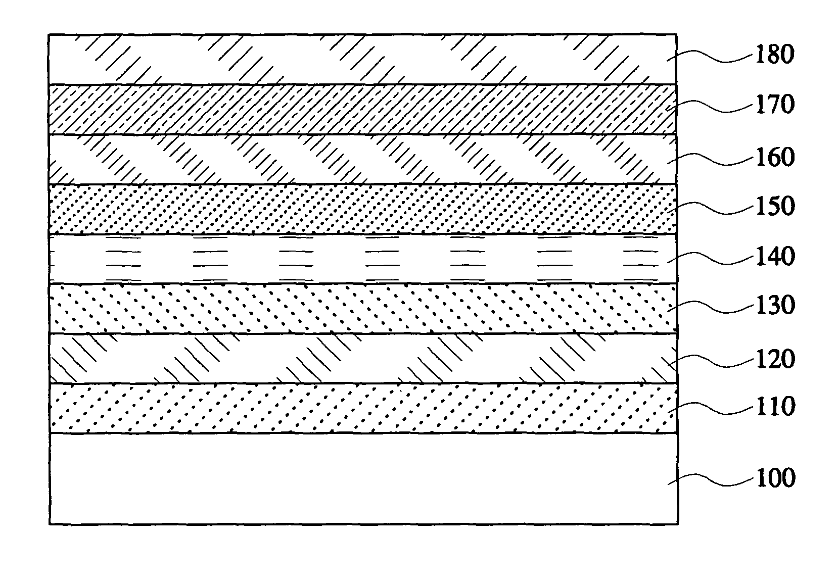
[0045]An anode was formed on a substrate using an ITO (Indium Tin Oxide). The substrate on which the ITO had been formed was subjected to cleaning, UV-O3 treating for 15 minutes, coating with a blended solution of BFE (obtained from Dow Chemical Company) with 5 wt % of 9,10-dicyanoanthracene (hereinafter, referred to as “DCA”) at a proper spin speed and at a thickness of 30 nm, and heat treating, and thus a hole injecting layer was formed. The electron affinity was 2.46 eV for the BFE, and 3.2 eV for the DCA.

[0046]A hole transporting layer, an emission layer, a hole blocking layer, an electron transporting layer, an electron injecting layer, and a cathode were sequentially deposited on the substrate on which the hole injecting layer had been formed, and the substrate was sealed using a moisture absorbent and a glass cover.

[0047]30 nm of IDE320 (obtained from IDEMITSU COMPANY) was used for the hole transporting layer, and 20 nm of IDE140 (obtained from IDEMITSU COMPANY) containing 6 ...

example 2

[0048]The organic light-emitting device was fabricated by the same method as Example 1, except that the hole transporting layer had not been formed.

[0049]Comparison 1

[0050]The organic light-emitting device was fabricated by the same method as Example 1, except that the hole injecting layer had been formed using BFE which was not blended with DCA.

[0051]Comparison 2

[0052]The organic light-emitting device was fabricated by the same method as Example 1, except that the hole injecting layer had been formed using BFE which was not blended with DCA, and that the hole transporting layer had not been formed.

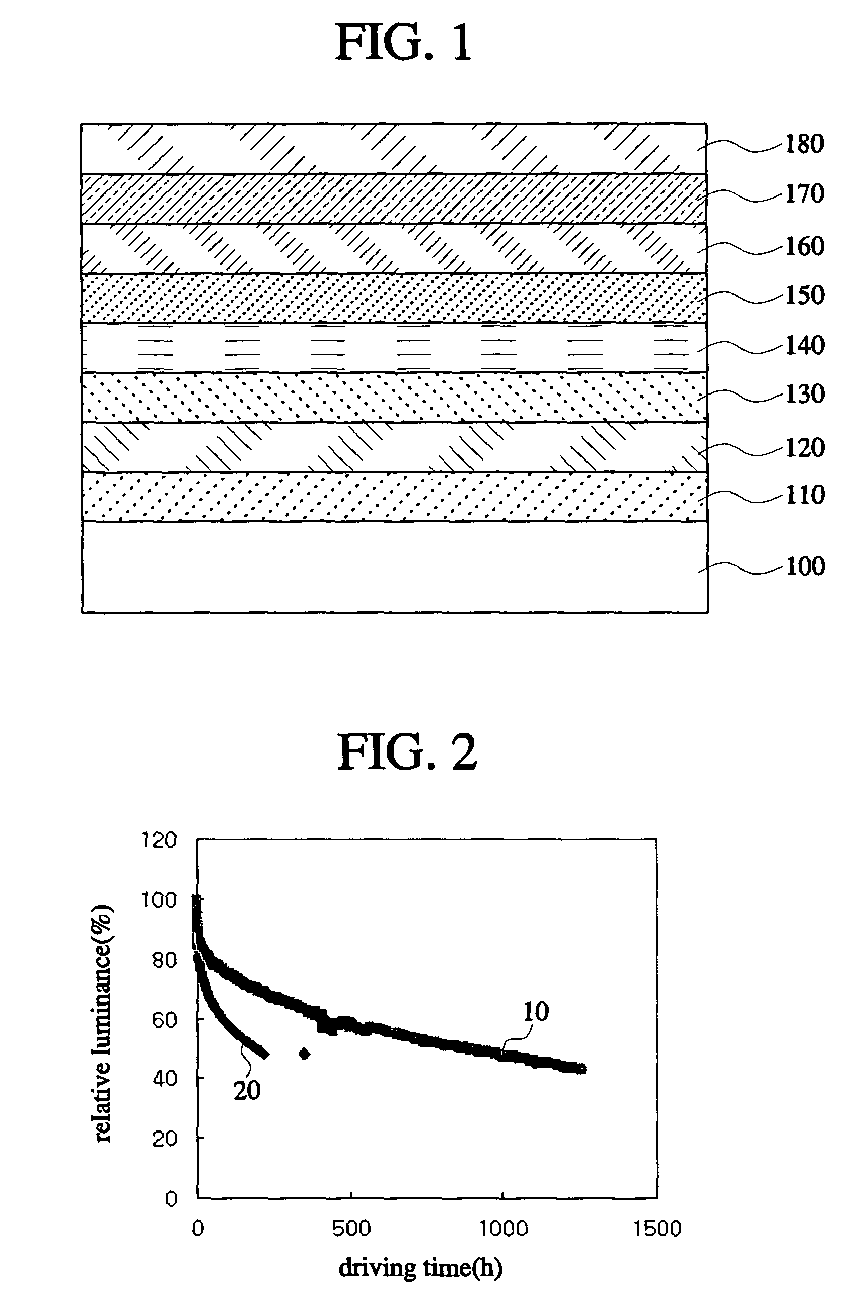
[0053]For the organic light-emitting devices fabricated according to Examples 1 and 2 as well as Comparisons 1 and 2, a driving voltage, a current density, and a luminous efficiency were measured respectively. The measured results are given in Table 1. The driving voltage and luminous efficiency were measured at a luminance of 200 nit, and the current density was measured at a voltage of ...

example 3

[0058]The organic light-emitting device was fabricated by the same method as Example 1, except that the blended solution of BFE with 5 wt % of DCA was coated at a thickness of 25 nm on the substrate, on which ITO had been formed, to form the hole injecting layer, and then the hole transporting layer having a thickness of 25 nm was formed on the hole injecting layer using IDE320.

[0059]Comparison 3

[0060]The organic light-emitting device was fabricated by the same method as Example 1, except that the BFE was not blended with DCA, and was coated at a thickness of 25 nm on the substrate, on which ITO had been formed, to form the hole injecting layer, and then the hole transporting layer having a thickness of 25 nm was formed on the hole injecting layer using IDE320.

[0061]For the organic light-emitting devices fabricated according to Example 3 and Comparison 3, a driving voltage, luminous efficiency and a half-lifetime were each measured. The measured results are given in Table 2. Further...


PUM

PropertyMeasurementUnit
Energyaaaaaaaaaa
Thicknessaaaaaaaaaa
Electron affinityaaaaaaaaaa

Abstract

An organic light-emitting device including an anode, a cathode, an emission layer interposed between the anode and the cathode, and at least one of the hole injecting layer and the hole transporting layer interposed between the anode and the emission layer, wherein the at least one of the hole injecting layer and the hole transporting layer includes a host material, and a dopant material as an electron acceptor, wherein the dopant material has an electron affinity greater than that of the host material by at least 0.1 eV.

Description

CROSS-REFERENCE TO RELATED APPLICATIONS[0001]This application claims the benefit of Korean Patent Application No. 2003-41250, filed Jun. 24, 2003, in the Korean Intellectual Property Office, the disclosure of which is incorporated herein by reference.BACKGROUND OF THE INVENTION[0002]1. Field of the Invention[0003]The present invention relates to an organic light-emitting device (OLED), and, more particularly, to an organic light-emitting device having a doped hole transporting layer (HTL) and / or a hole injecting layer (HIL).[0004]2. Description of the Related Art[0005]An organic light-emitting device, such as a self-emissive display, has an ideal structure in that it is compact and light-weight and has simple components and processes. The OLED also has several other advantages, such as the capability to secure high definition and a wide viewing angle, the capability to realize a superb moving picture and a high contrast, and an electrical characteristic suitable for a mobile device ...

Claims


Application Information

Patent Timeline
IPC IPC(8): H01J1/62H05B33/12H05B33/26C09K11/06H01L51/50H05B33/20
CPCH01L51/5052H01L51/5088Y10S428/917H10K50/155H10K50/17H05B33/26
Inventor SUH, MIN CHULYANG, NAM-CHOULCHIN, BYUNG-DOOKIM, MU-HYUNLEE, SEONG-TAEK
Owner SAMSUNG DISPLAY CO LTD
Why Eureka
Try Eureka