

Semiconductor device
a technology of semiconductor devices and sealing rings, which is applied in the details of semiconductor devices, semiconductor/solid-state devices, electrical appliances, etc., can solve the problems of deteriorating resistance to absorbed moisture of semiconductor devices, negatively affecting the circuit formation region, etc., and achieves the effect of improving the reliability of semiconductor devices and preventing cracking
- Summary
- Abstract
- Description
- Claims
- Application Information
AI Technical Summary
Benefits of technology
Problems solved by technology
Method used
Image

Examples
first embodiment
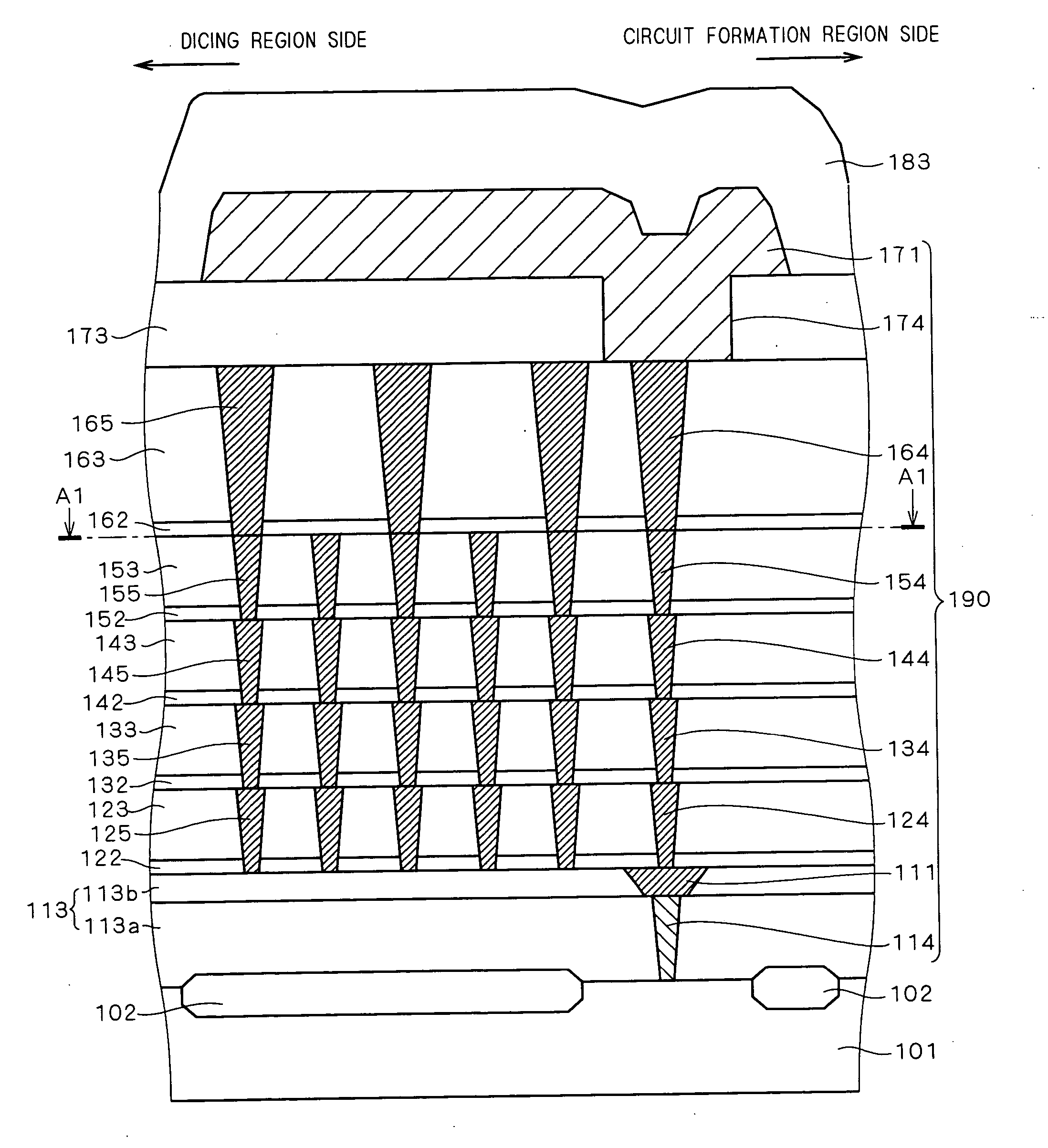
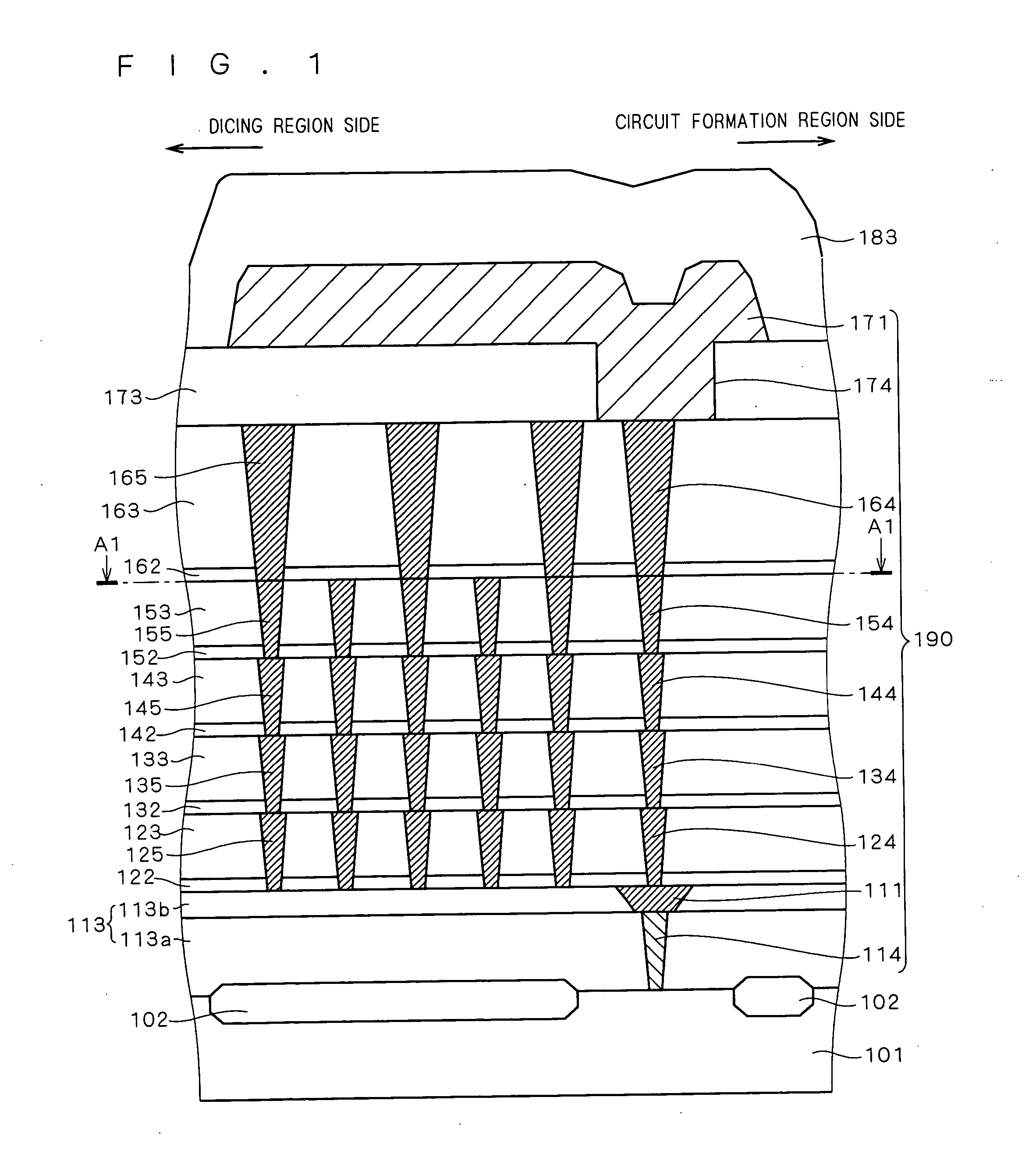
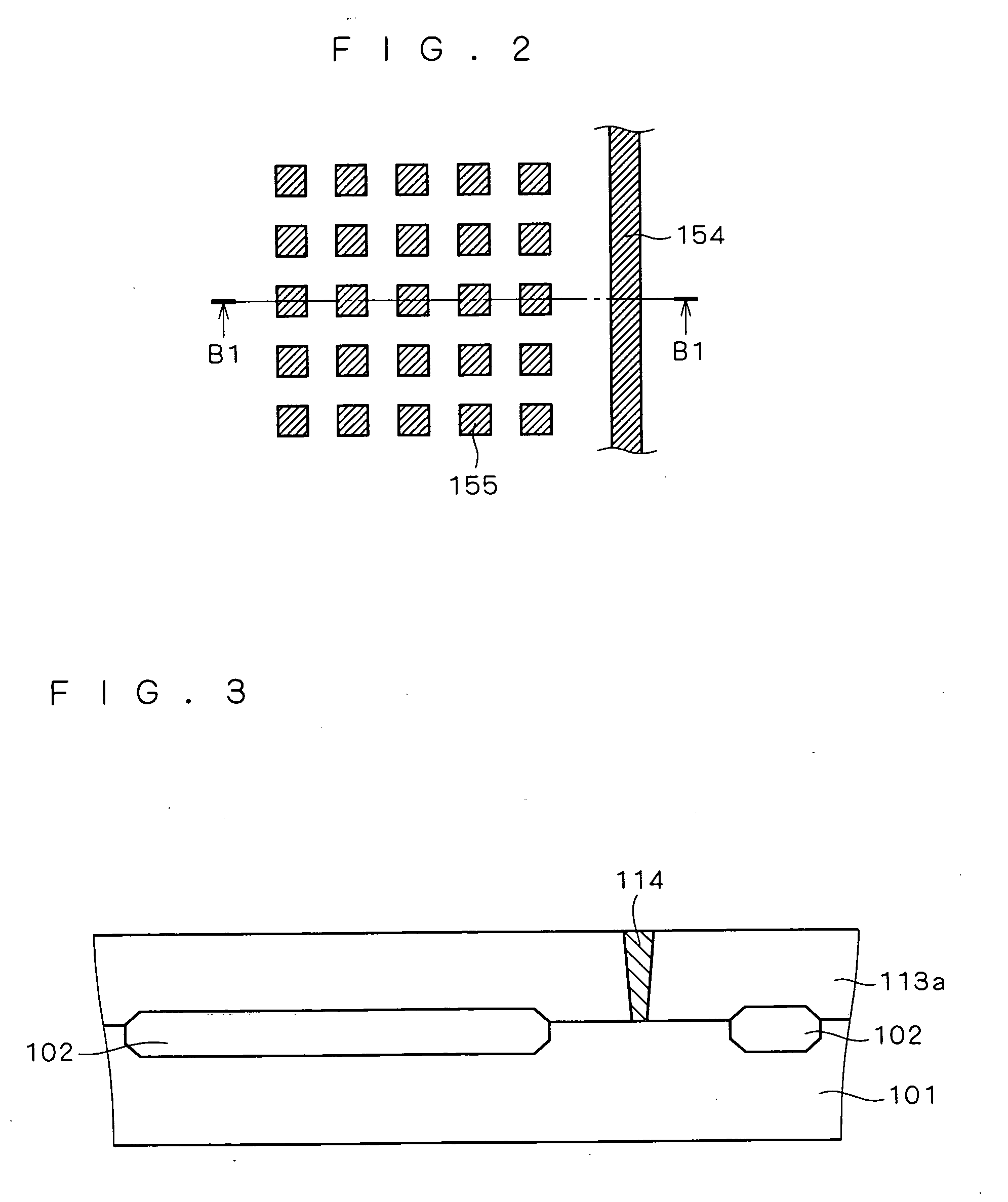
[0052]FIG. 1 shows a configuration of a semiconductor device according to a first embodiment, which is an enlarged sectional view of a region where a seal ring is formed. FIG. 2 is a top view of the semiconductor device viewed along line A1-A1 ofFIG. 1. In addition, FIG. 1 is also a sectional view taken along line B1-B1 of FIG. 2. A circuit formation region is to the right and a dicing region is to the left of the region shown in FIG. 1, respectively.
[0053] Here, semiconductor chips are aligned in a matrix on a semiconductor wafer and the respective semiconductor chips are separated by a dicing region. A circuit formation region is formed in a semiconductor chip and a seal ring is placed around the circuit formation region. Namely, the seal ring is formed to surround the circuit formation region. FIG. 1 shows an end surface of such a semiconductor chip and, also, shows the vicinity of an edge (region where a seal ring is formed) of a semiconductor chip.
[0054] In the same figure, t...
second embodiment
[0095]FIG. 10 shows a configuration of a semiconductor device according to a second embodiment, which is an enlarged sectional view of a region where a seal ring is formed. FIG. 11 is a top view of the semiconductor device as viewed along line A2-A2 of FIG. 10. In addition, FIG. 10 is a sectional view of the semiconductor device taken along line B2-B2 of FIG. 11. In this embodiment, dummy metals and interconnecting layers are additionally formed in each layer. In the following description, the same symbols are attached to components that are the same as those in the first embodiment, and the description thereof is omitted.
[0096] A dummy metal 116 is formed in the same plane as an interconnecting layer 111. In addition, dummy vias 125 are formed on the dummy metal 116. A dummy metal 126 is formed on the dummy vias 125. Dummy metals 136, 146, 156 and 166 are formed on dummy vias 135, 145, 155 and 165, respectively. In addition, interconnecting layers 121, 131, 141, 151 and 161 are fo...
third embodiment
[0117]FIG. 19 shows a configuration of a semiconductor device according to a third embodiment, which is an enlarged sectional view of a region where a seal ring is formed. FIG. 20 is a top view of the semiconductor device as viewed along line A3-A3 of FIG. 19. In addition, FIG. 19 is a sectional view of the semiconductor device taken along line B3-B3 of FIG. 20. The same symbols are attached to components that are the same as those in the first embodiment, and the description thereof is omitted.
[0118] In the semiconductor device according to this embodiment, dummy vias 155 are arranged in such a manner that they are aligned in zigzag pattern, as shown in the top view of FIG. 20. Namely, dummy vias formed in adjacent columns are shifted by half a pitch from each other. In other words, the dummy vias 155 are arranged along a plurality of columns in a plan view, and the dummy vias 155 which are arranged in adjacent columns are alternately arranged so as to be aligned in zigzag pattern...
PUM
 Abstract
Description
Claims
Application Information