Methods of making electromechanical three-trace junction devices

Inactive Publication Date: 2005-12-22
NANTERO
View PDF42 Cites 36 Cited by
  • Summary
  • Abstract
  • Description
  • Claims
  • Application Information

AI Technical Summary

Problems solved by technology

ROM is relatively low cost but cannot be rewritten.
EEPROM (or “Flash”) is inexpensive, and has low power consumption but has long (millisecond) write cycles and low relative speed in comparison to DRAM or SRAM.
Flash also has a finite number of read/write cycles leading to low long-term reliability.
DRAM stores charges on transistor gates that act as capacitors, but its need to be electrically refreshed every few milliseconds complicates system design by requiring separate circuitry to “refresh” the memory contents before the capacitors discharge.
SRAM does not need to be refreshed and is fast relative to DRAM, but has lower density and is more expensive relative to DRAM.
Both SRAM and DRAM are volatile, meaning that if power to the memory is interrupted the memory will lose the information stored in the memory cells.
As the discussion above indicates, conventional memory solutions fail to possess all the desired characteristics.
Existing technologies that are nonvolatile are not randomly accessible and have low density, high cost, and limited ability to allow multiple writes with high reliability of circuit function.
Meanwhile, existing technologies that are volatile complicat

Method used


Image

  • Methods of making electromechanical three-trace junction devices
  • Methods of making electromechanical three-trace junction devices
  • Methods of making electromechanical three-trace junction devices

Examples


Embodiment Construction

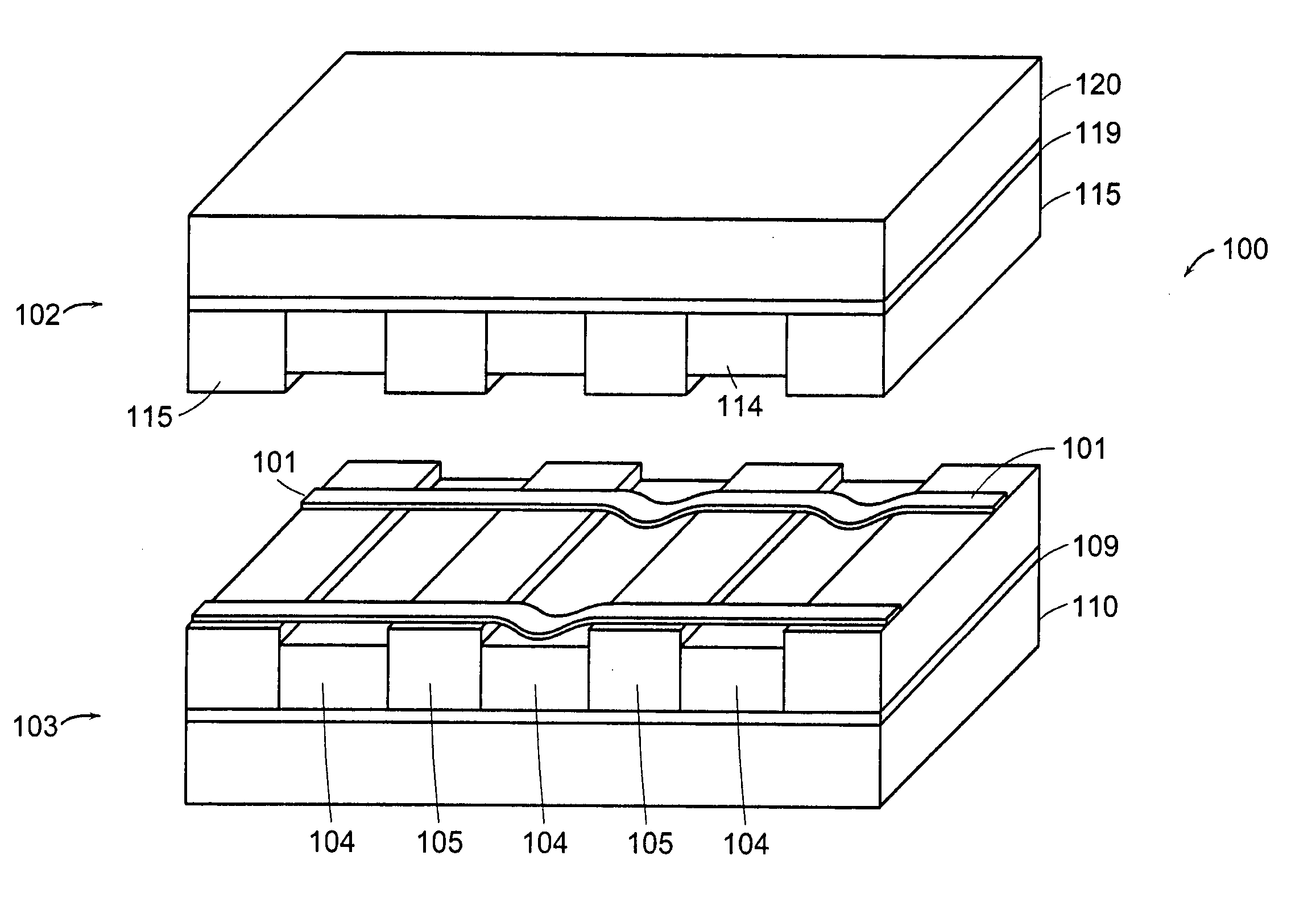
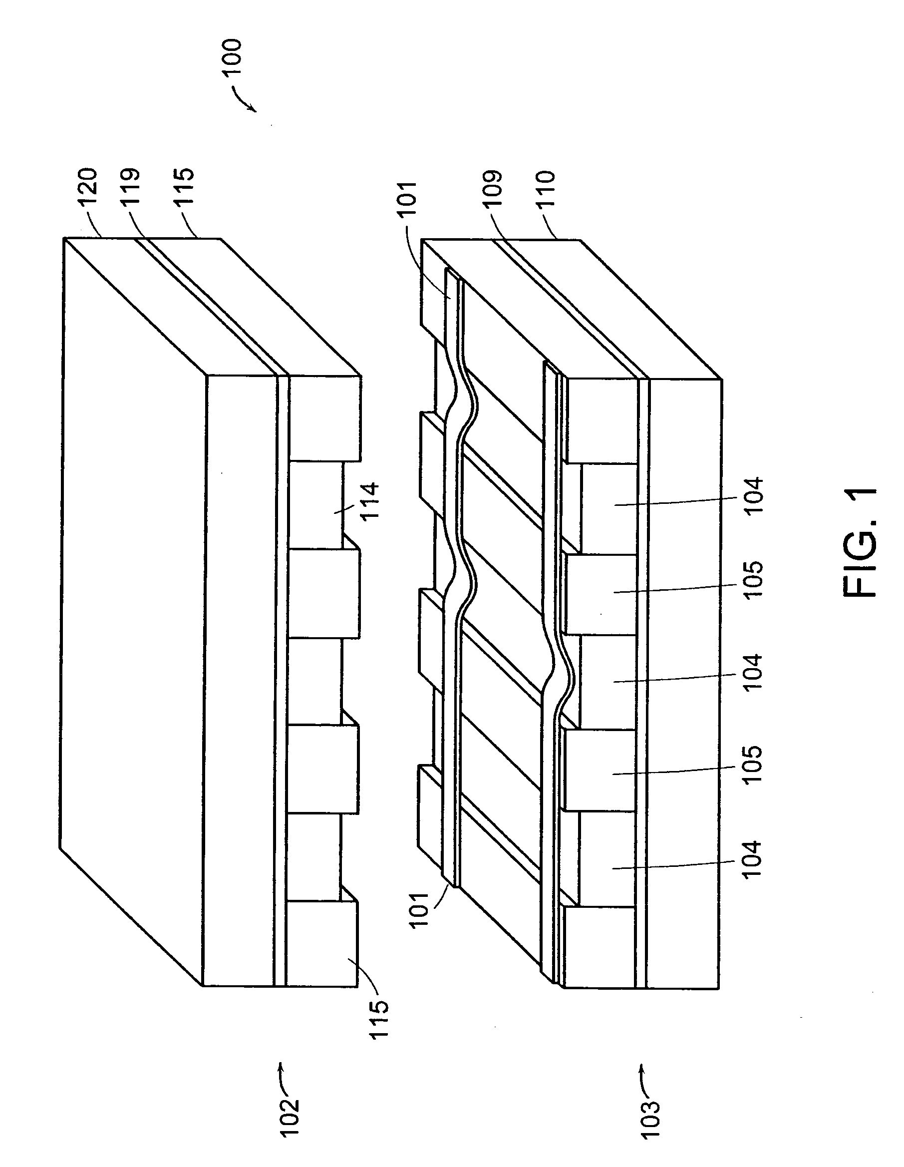
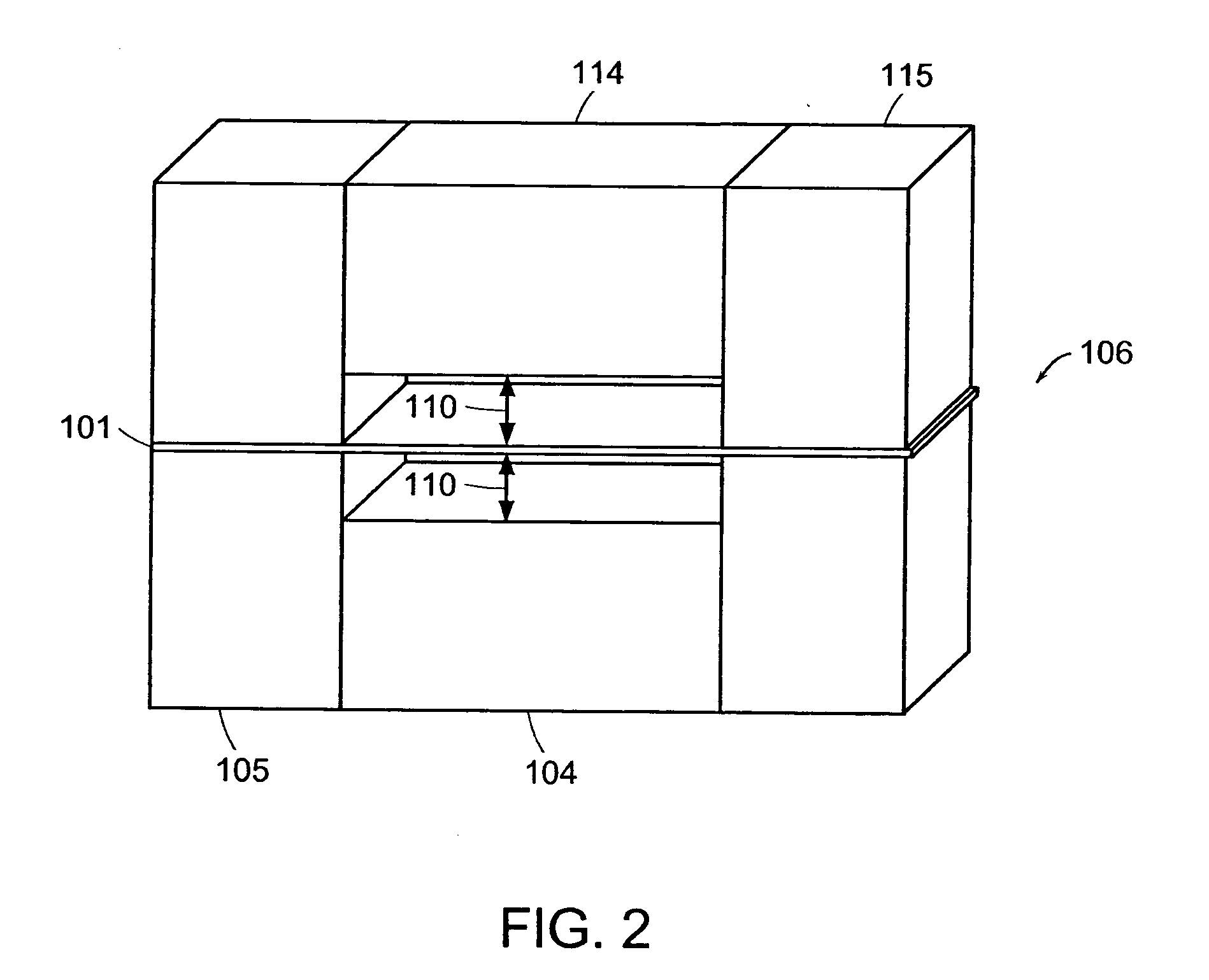
[0032] Preferred embodiments of the invention provide new electromechanical circuit elements and methods of making the same. In particular, three trace nanotube-technology devices are shown and methods of making same are described. As will be explained below, the use of three traces (1) facilitates tristable logic that may achieve higher memory storage and / or information densities, (2) improves reliability and speed of switching a given element or cell, and (3) improves fault tolerance of an element or cell. Moreover, certain embodiments effectively enclose the three-trace junctions, facilitating their use, fabrication, and distribution, especially in the case of hybrid circuits.

[0033] In short, preferred embodiments of the present invention include electromechanical circuit junctions formed from at least three crossing junctions, only one of which needs to be an electromechanically responsive trace. Though the electromechanically responsive trace may be formed from a carbon nanotu...


PUM


Abstract

Methods of producing an electromechanical circuit element are described. A lower structure having lower support structures and a lower electrically conductive element is provided. A nanotube ribbon (or other electromechanically responsive element) is formed on an upper surface of the lower structure so as to contact the lower support structures. An upper structure is provided over the nanotube ribbon. The upper structure includes upper support structures and an upper electrically conductive element. In some arrangements, the upper and lower electrically conductive elements are in vertical alignment, but in some arrangements they are not.

Description

CROSS REFERENCE TO RELATED APPLICATIONS [0001] This application is a continuation of and claims priority under 35 U.S.C. §120 to U.S. patent application Ser. No. 10 / 824,679 filed on Apr. 15, 2004, entitled Methods Of Making Electromechanical Three-Trace Junction Devices, which is a continuation of U.S. patent application Ser. No. 10 / 033,032 filed on Dec. 28, 2001, entitled Methods Of Making Electromechanical Three-Trace Junction Devices. [0002] This application is related to the following applications, the contents of which are incorporated herein in their entirety by reference: [0003] U.S. patent application Ser. No. 09 / 915,093 filed Jul. 25, 2001 (now U.S. Pat. No. 6,919,592) entitled Electromechanical Memory Array Using Nanotube Ribbons And Method For Making Same; [0004] U.S. patent application Ser. No. 09 / 915,173 filed Jul. 25, 2001 (now U.S. Pat. No. 6,643,15) entitled Electromechanical Memory Having Cell Selection Circuitry Constructed With Nanotube Technology; and [0005] U.S....

Claims


Application Information

Patent Timeline
IPC IPC(8): B81B3/00G11C11/34G11C13/02H01H59/00H01L21/768
CPCB81C1/00142B81C2201/019B82Y10/00G11C13/025Y10S977/734G11C2213/16G11C2213/81H01H1/0094H01L21/76838G11C23/00
Inventor RUECKES, THOMASSEGAL, BRENT M.BROCK, DARREN K.
Owner NANTERO
Why Eureka
Try Eureka