Ultra-linear multi-channel field effect transistor

a field effect transistor and multi-channel technology, applied in the field of field effect transistors, can solve the problems of non-linearity, limit the dynamic range of amplifiers, limit the application of lower frequencies, etc., and achieve the effect of constant cut-off frequency variation and sharp impurity gradien

Inactive Publication Date: 2005-12-29
EPITAXIAL TECH
View PDF9 Cites 57 Cited by
  • Summary
  • Abstract
  • Description
  • Claims
  • Application Information

AI Technical Summary

Benefits of technology

[0013] An object of this invention is to obtain a linear dc ID variation as a function of VGS and a constant transconductance variation in the characteristics of a FET over a wide range of VGS. Another object of this invention is to obtain a sharp impurity gradient in the channel of a FET. Still another object of this ...

Problems solved by technology

This square-law relationship causes non-linearity (harmonic distortion) and limits the dynamic range of amplifiers.
Further, the lower mobilities of the HFET limit its applications to l...

Method used


Image

  • Ultra-linear multi-channel field effect transistor
  • Ultra-linear multi-channel field effect transistor
  • Ultra-linear multi-channel field effect transistor

Examples


Embodiment Construction

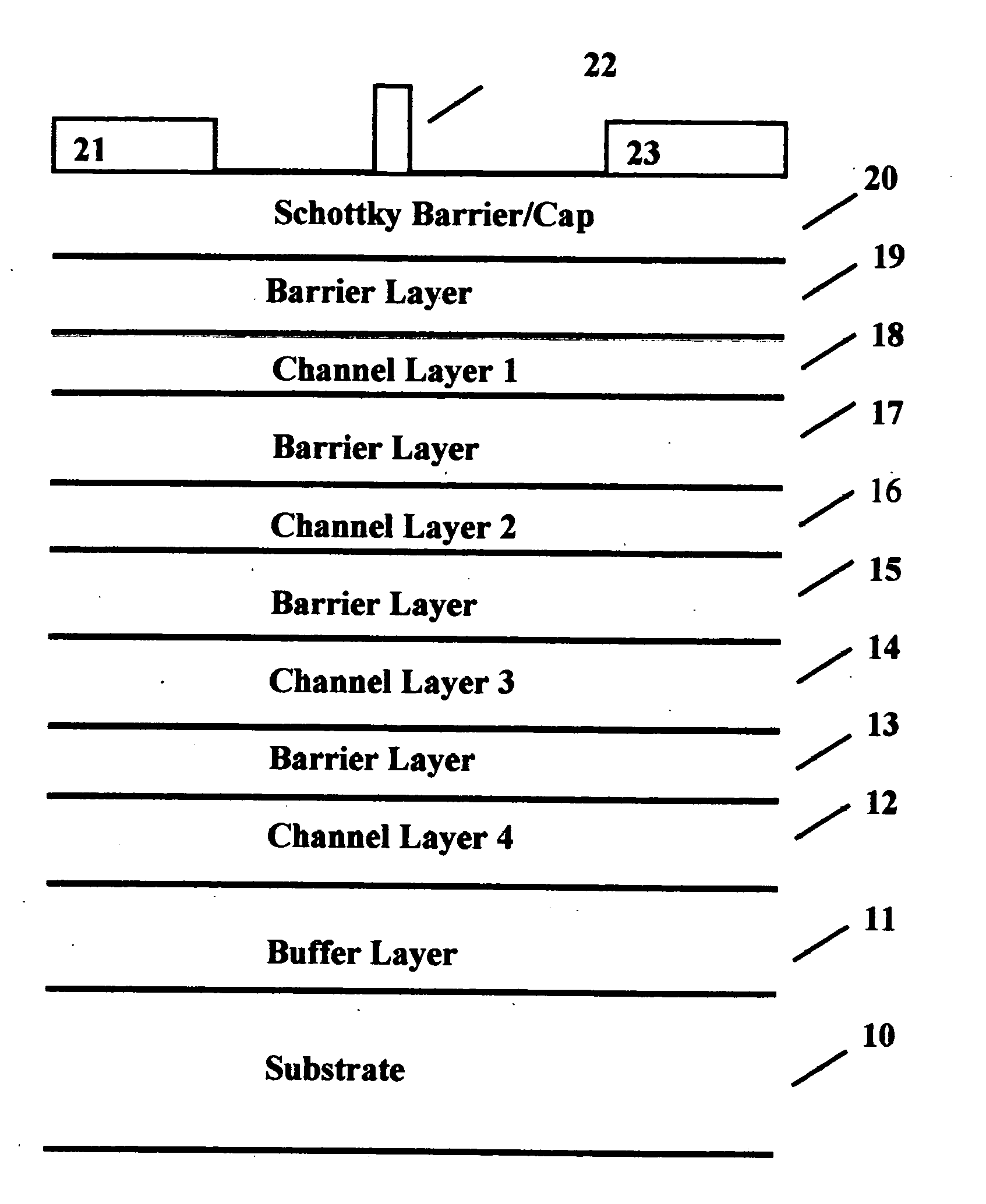
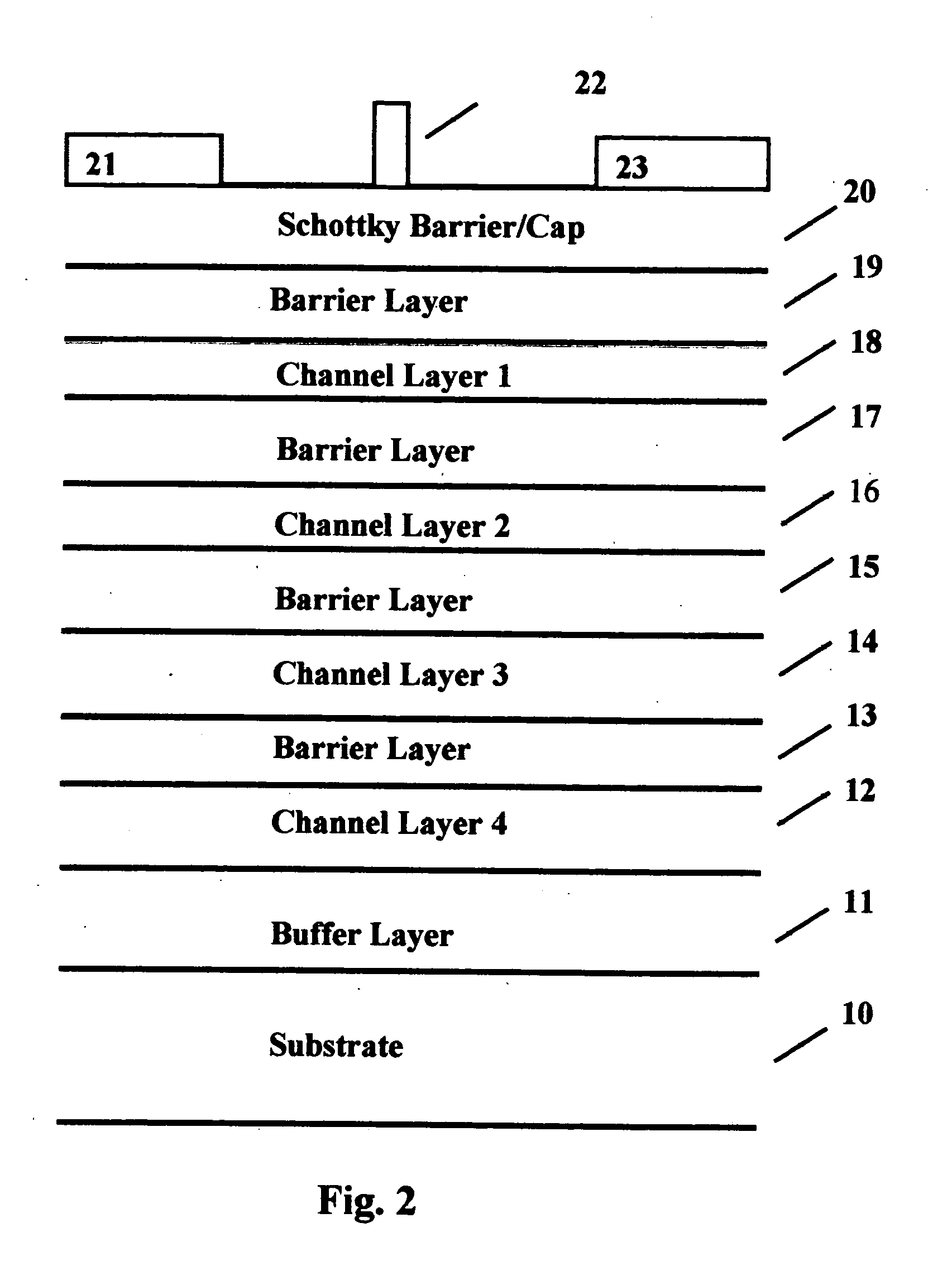
[0028]FIG. 2 shows the basic structure of multiple channel heterojunction field effect transistor of the present invention. The structure has a substrate 10 and an undoped buffer layer 12 deposited on the substrate. The multiple channel HFET is formed with alternate undoped barrier layers 12, 14, 16, 18 of a first kind of semiconductor and doped channel layers 13, 15, 17 of a second kind of semiconductor. The two kinds of different semiconductor material form heterojunctions in the multiple channels. Another layer 20 is used to cap the multiple channels. An optional oxidation barrier is inserted (e.g. to protect layers such as AlSb, AlAsSb) between the layer 19 and cap 20. A thin layer of undoped GaAs cap can be used to improve the uniformity of the threshold voltage of the HFET. Alternately doped GaInAs (or InAs) can be used as the cap, but requires recess etching before forming metal gate. Over the layer 20, the source 21, gate 22 and drain 23 are formed laterally. Ohmic contacts ...


PUM


Abstract

Alternate layers of wide band gap and narrow band gaps of different kinds of semiconductors are used to form multiple channels of a FET. The channels are doped or formed as 2-DEG/2-DHG in narrow band semiconductor by charge supply layer in the wide band gap semiconductor. The different kinds of semiconductors form heterojunctions to confine the electrons/holes in separate thin spikes layers. A number of spikes (3-10 nm thick) of different doped or 2-DEG/2-DHG concentrations in various channels can result in overall electron concentration gradient such as a 1/x3 electron/hole concentrations profile. Such an electron/hole concentration gradient can result in a linear variation of drain current with voltage to obtain a wide dynamic range.

Description

[0001] This application is a continuation of application Ser. No. 10 / 176,787, filed Jun. 24, 2002 (pending).BACKGROUND OF THE INVENTION [0002] (1) Field of the Invention [0003] This invention relates to field effect transistors, in particular to a multiple channel, ultra-linear field effect transistors. [0004] (2) Description of the Related Art [0005] A field effect transistor (FET) normally is a square-law device. In the current saturation of the drain current (ID) vs gate-to-source voltage (VGS) of the characteristic of a FET, the basic relationship is given as: ID=K(VGS−Vt)2   (1) where K is a transconductance parameter, and Vt is the threshold voltage. When an input voltage is applied as a change in VGS, the output current, which appears as the change in ID, does not vary linearly with VGS. This square-law relationship causes non-linearity (harmonic distortion) and limits the dynamic range of amplifiers. [0006] In equation (1), the threshold voltage Vt is assumed to be constant...

Claims


Application Information

Patent Timeline
IPC IPC(8): H01L29/10H01L29/778H01L29/812H01L31/0328
CPCB82Y10/00H01L29/1029H01L29/2003H01L29/802H01L29/7785
Inventor FATHIMULLA, AYUB MOHAMMEDHIER, HARRY STEPHENAINA, OLALEYE ADETORD
Owner EPITAXIAL TECH
Why Eureka
Try Eureka