Method for fabricating semiconductor packages

a technology of semiconductor packages and fabrication methods, applied in semiconductor devices, semiconductor/solid-state device details, electrical devices, etc., can solve the problems of material waste, significant drawbacks in the fabrication process, increase material and fabrication costs, etc., and achieve easy separation, poor adhesion, and avoidance of material waste

Active Publication Date: 2005-12-29
SILICONWARE PRECISION IND CO LTD
View PDF5 Cites 11 Cited by
  • Summary
  • Abstract
  • Description
  • Claims
  • Application Information

AI Technical Summary

Benefits of technology

[0017] The foregoing metal carrier can be made of a copper (Cu) material, and a surface thereof is plated with a metal layer that is poorly adhesive to the encapsulant. The metal layer can be made of a metal material such as gold (Au), nickel (Ni), or chromium (Cr), etc. By virtue of the poor adhesion between the plated metal layer and the encapsulant, the package unit can be easily separated from the metal carrier, thereby providing convenience of fabrication.
[0018] Therefore, according to the foregoing arrangement, the length and width of the substrate in the present invention can be perfectly matched with the predetermined length and width of the package, such that no edge portion of the substrate would be cut off during singulation and a material waste is avoided. Furthermore, the resin-flash problem during molding and the mold-releasing problem can be solved by simply sealing the gaps between the substrates and the carrier, and allowing coverage of a mold cavity used for forming the encapsulant to be larger in length and width than the size of the opening. This does not require the size of the substrate to be undesirably increased and thus eliminates the drawbacks in the prior art.

Problems solved by technology

However, the FCBGA semiconductor package still causes significant drawbacks in its fabrication processes.
The discarded extra portions of the substrate 70 not only cause a material waste but also increase the material and fabrication costs.
However, such design obviously increases the size of the substrate 70.
Therefore, an additional portion of 1.2 mm that is to be eventually cut off is included respectively in the length and width of the substrate 70, which thus increases materials required for the substrate 70 and also increases the overall fabrication cost of the package (the substrate cost is generally more than 60% of the overall cost of the flip-chip package).
This causes not only a waste of utilization of the substrate but also 15˜20% increase in the overall cost.
The above problem leads to significant difficulty in the fabrication of the FCBGA semiconductor package.
Although the molding process of forming the encapsulant 73 is an essential step for fabricating the package, it would effectively increase the size and material cost of the substrate 70 and is not advantageous for mass production.
This thus sets a bottleneck in development of the FCBGA semiconductor package.

Method used


Image

  • Method for fabricating semiconductor packages
  • Method for fabricating semiconductor packages
  • Method for fabricating semiconductor packages

Examples


first preferred embodiment

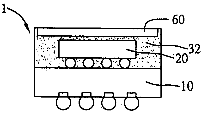
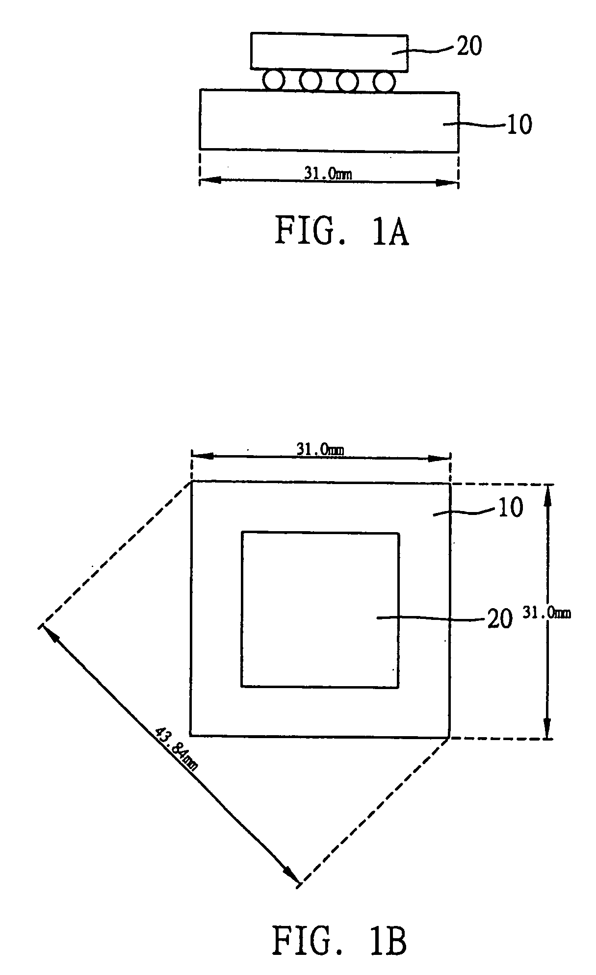
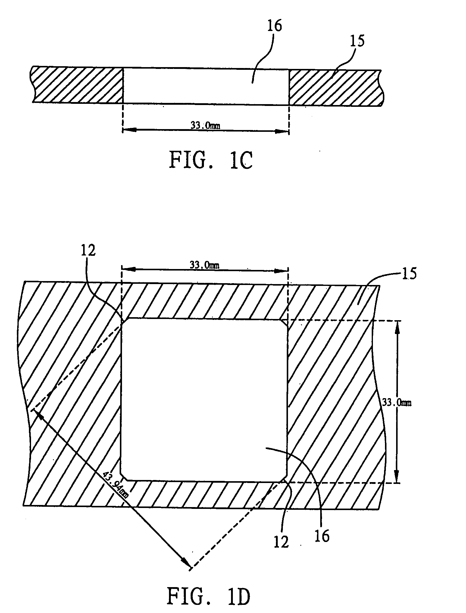
[0031]FIGS. 1A to 1K show a method for fabricating semiconductor packages according to a first preferred embodiment of the present invention. First referring to FIG. 1A, a plurality of build-up substrates 10 (only one is shown) each carrying a chip 20 thereon are prepared. The length and width of each of the substrates 10 are approximately equal to predetermined length and width of the final semiconductor package 1 (shown in FIG. 1K) respectively. In this embodiment, the predetermined dimensions of the semiconductor package 1 after singulation are 31 mm×31 mm in length and width, such that the length and width of the substrate 10 are also sized as 31 mm×31 mm, and a diagonal of the substrate 10 is 43.84 mm long as shown in FIG. 1B. Referring to FIG. 1C, a substrate carrier 15 having a plurality of rectangular openings 16 (only one is shown) is prepared. As shown in FIG. 1D, a protruded portion 12 is provided at each corner position of each of the openings 16, and a distance between ...

second preferred embodiment

[0038] Apart from the carrier 15 being made of the organic insulating material such as FR4, FR5 or BT, a metal carrier having a metal layer plated on a surface thereof can also be used in the present invention. The metal layer is made of a material that is poorly adhesive to the encapsulant 32. FIGS. 4A to 4J show a method for fabricating semiconductor packages by using the metal carrier. In this embodiment, the predetermined dimensions of the semiconductor package 1, the dimensions of the substrate 10 and the size of openings 46 of the metal carrier 45 are all consistent with those in the foregoing first embodiment. Only the material used for the carrier 45 and some of the fabrication processes in this embodiment differ from those of the first embodiment.

[0039] First referring to FIG. 4A, a plurality of build-up substrates 10 (only one is shown) each carrying a chip 20 thereon are prepared. The length and width of each of the substrates 10 are made equal to the predetermined lengt...

third preferred embodiment

[0042] In the foregoing embodiments, the molding process is performed to allow the encapsulant 32 to encapsulate the chip 20 (flip chip) and solder bumps for electrically connecting the flip chip 20 to the substrate 10. However, in this third embodiment, referring to FIG. 5, an underfilling process is carried out to use an underfill material 51 such as epoxy resin to encapsulate the solder bumps 50 and fill a gap between the flip chip 20 and the substrate 10 prior to the molding process. This can further enhance the mechanical strength of the solder bumps 50 and electrical performances of the semiconductor package 1.


PUM


Abstract

A method for fabricating semiconductor packages is proposed. A plurality of substrates are prepared each having a chip thereon. Length and width of each substrate are equal to predetermined length and width of the semiconductor package. A carrier having a plurality of openings is prepared. A protruded portion is formed at each corner of each opening, wherein a distance between two diagonal protruded portions is slightly larger than that between two diagonal corners of the substrate. The substrates are fixed in the openings of the carrier by means of the protruded portions, and gaps between the substrates and the carrier are sealed. An encapsulant is formed over each opening to encapsulate the corresponding chip by a molding process. An area on the carrier covered by the encapsulant is larger in length and width than the opening. A plurality of the semiconductor packages are formed after performing mold-releasing and singulation processes.

Description

FIELD OF THE INVENTION [0001] The present invention relates to methods for fabricating semiconductor packages, and more particularly, to a fabrication method of ball grid array semiconductor packages using a substrate carrier. BACKGROUND OF THE INVENTION [0002] A flip-chip ball grid array (FCBGA) semiconductor package is a package structure comprising both a flip chip and a ball grid array, wherein an active surface of at least one chip is electrically connected to a surface of a substrate via a plurality of solder bumps in a flip-chip manner, and a plurality of solder balls are implanted on an opposite surface of the substrate to serve as input / output (I / O) connections. This package structure yields significant advantages to effectively decrease the package size, reduce resistance and improve electrical performances without using conventional bonding wires, thereby preventing decay of signals during transmission. Therefore, the FCBGA semiconductor package has become a mainstream pa...

Claims


Application Information

Patent Timeline
Patent Type & Authority Applications(United States)
IPC IPC(8): H01L21/44H01L21/48H01L21/50H01L21/56H01L21/60H01L23/31H01L23/433
CPCH01L21/4846H01L2924/014H01L21/565H01L23/3128H01L23/4334H01L24/81H01L24/97H01L2224/16H01L2224/73253H01L2224/81801H01L2224/83102H01L2224/92125H01L2224/97H01L2924/01029H01L2924/01079H01L2924/15311H01L2924/18161H01L21/50H01L2924/01033H01L2924/01024H01L2924/01006H01L2924/01005H01L2924/181H01L2924/00012
Inventor LIN, YING-RENTSAI, HO-YIHUANG, CHIEN-PING
Owner SILICONWARE PRECISION IND CO LTD
Why Eureka
Try Eureka