Methods and devices for forming nanostructure monolayers and devices including such monolayers

a nanostructure monolayer and nanotechnology technology, applied in the field of nanotechnology, can solve problems such as difficulty in scaling up to form large numbers

Active Publication Date: 2005-12-29
WODEN TECH INC
View PDF53 Cites 216 Cited by
  • Summary
  • Abstract
  • Description
  • Claims
  • Application Information

AI Technical Summary

Benefits of technology

[0042] Part or substantially all the solvent is evaporated. A rate of evaporation of the solvent can be controlled, e.g., to control array formation. For example, slow evaporation of the solvent gra

Problems solved by technology

However, the former technique is difficult to scale up to form large numbers of monolayers, and the latter technique produces a layer

Method used


Image

  • Methods and devices for forming nanostructure monolayers and devices including such monolayers
  • Methods and devices for forming nanostructure monolayers and devices including such monolayers
  • Methods and devices for forming nanostructure monolayers and devices including such monolayers

Examples


Embodiment Construction

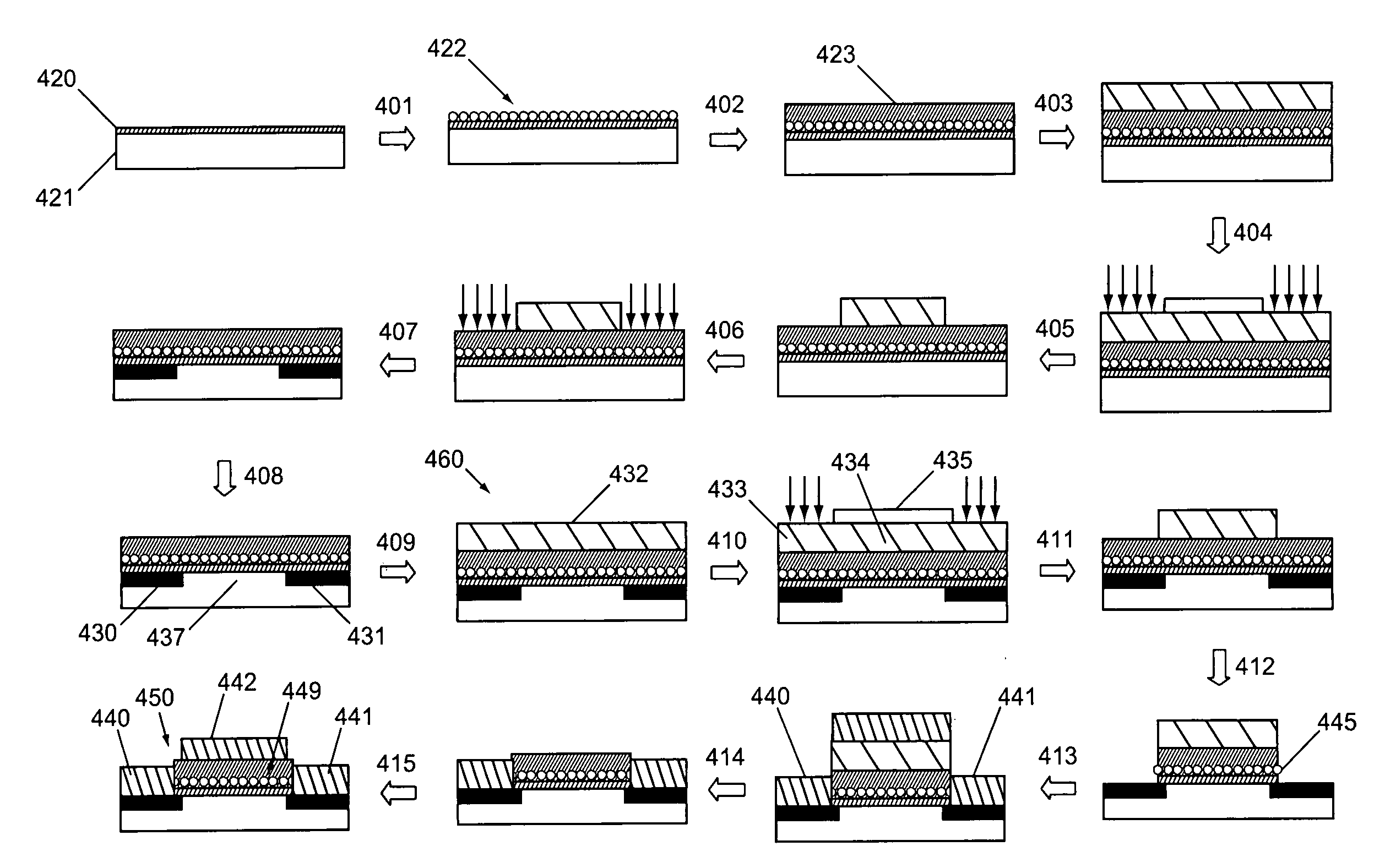
[0084] In one aspect, the invention provides methods for forming nanostructure arrays, e.g., ordered or disordered monolayer arrays of nanostructures. The arrays are optionally formed at predetermined positions and / or have predetermined dimensions. Devices related to the methods are also provided, as are devices including nanostructure arrays. For example, in one aspect, the invention provides memory devices including small monolayer arrays of nanostructures.

Monolayer Formation on Chemical Coatings

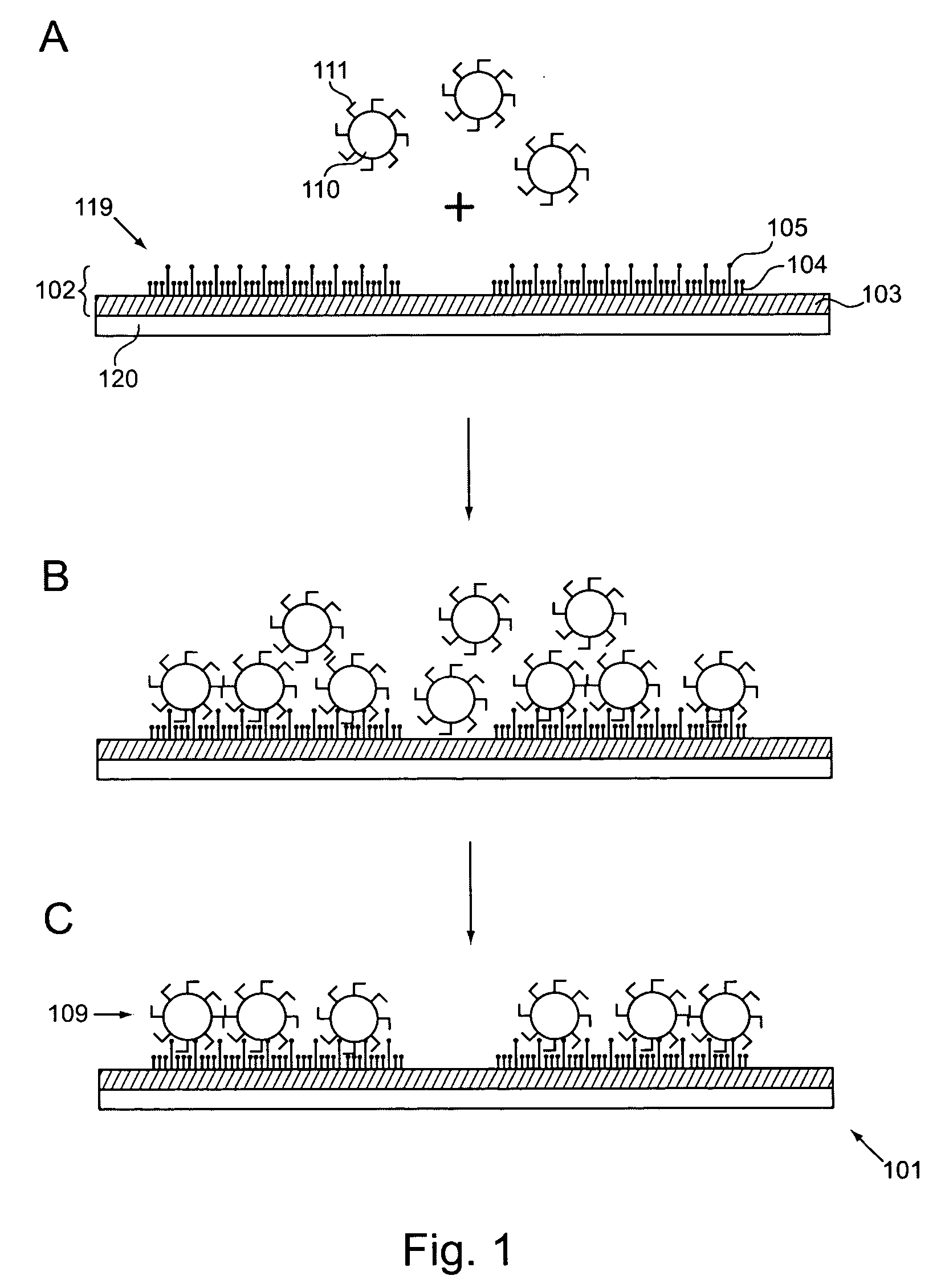
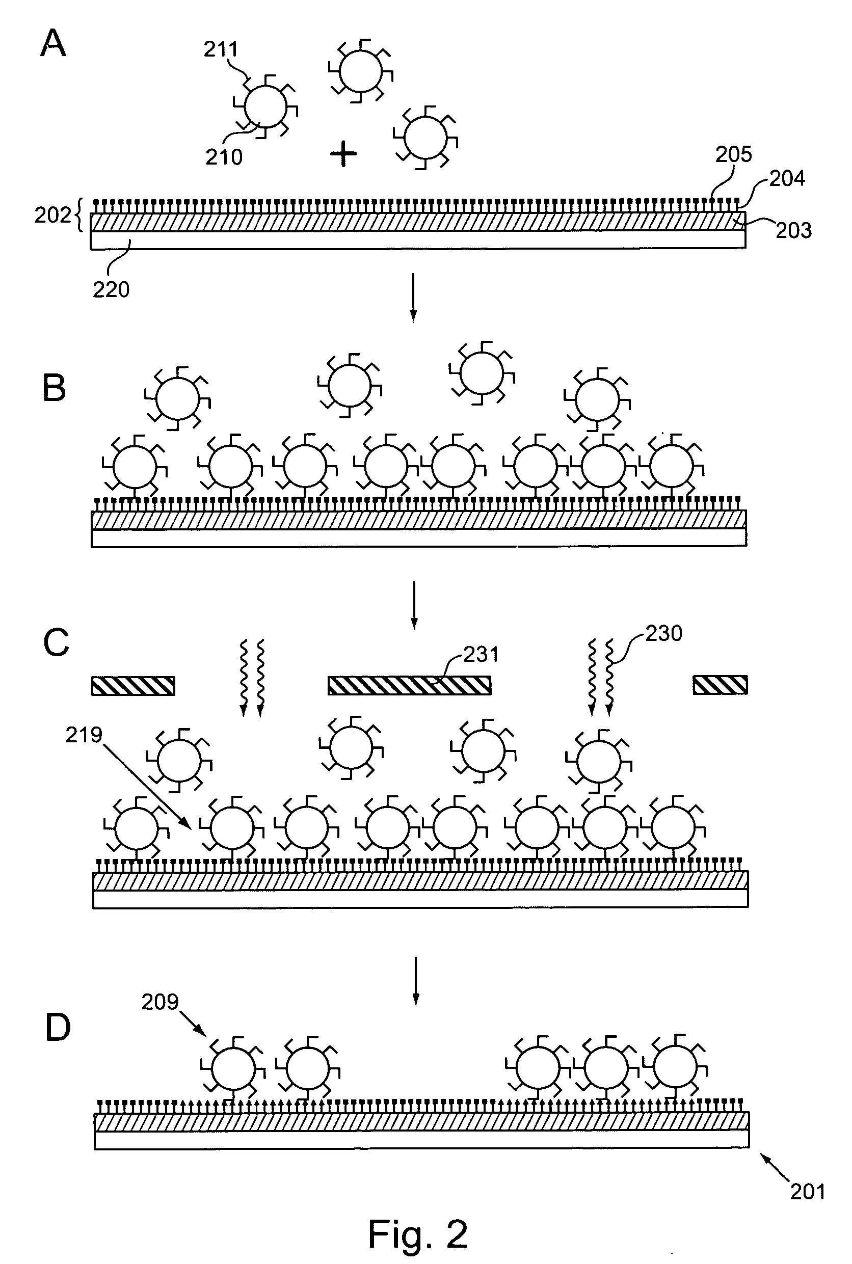
[0085] A surface on which a nanostructure array is to be formed can be coated with a chemical composition, e.g., a composition having a higher affinity for the nanostructures than the surface itself does. Such a coating can, e.g., facilitate adhesion of the nanostructures to the surface and can thus facilitate formation of the monolayer.

[0086] Thus, one general class of embodiments provides methods for forming a nanostructure array. In the methods, a first layer is provided and coated ...


PUM


Abstract

Methods for forming or patterning nanostructure arrays are provided. The methods involve formation of arrays on coatings comprising nanostructure association groups, patterning using resist, and/or use of devices that facilitate array formation. Related devices for forming nanostructure arrays are also provided, as are devices including nanostructure arrays (e.g., memory devices).

Description

CROSS-REFERENCE TO RELATED APPLICATIONS [0001] This application is a non-provisional utility patent application claiming priority to and benefit of the following prior provisional patent applications: U.S. Ser. No. 60 / 671,134, filed Apr. 13, 2005, entitled “METHODS AND DEVICES FOR FORMING NANOSTRUCTURE MONOLAYERS AND DEVICES INCLUDING SUCH MONOLAYERS” by David L. Heald, et al., U.S. Ser. No. 60 / 578,236, filed Jun. 8, 2004, entitled “POST-DEPOSITION ENCAPSULATION OF NANOCRYSTALS: COMPOSITIONS, DEVICES AND SYSTEMS INCORPORATING SAME” by Jeffery A. Whiteford et al., and U.S. Ser. No. 60 / 632,570, filed Nov. 30, 2004, entitled “POST-DEPOSITION ENCAPSULATION OF NANOSTRUCTURES: COMPOSITIONS, DEVICES AND SYSTEMS INCORPORATING SAME” by Jeffery A. Whiteford et al., each of which is incorporated herein by reference in its entirety for all purposes.FIELD OF THE INVENTION [0002] This invention relates primarily to the field of nanotechnology. More specifically, the invention pertains to methods ...

Claims


Application Information

Patent Timeline
IPC IPC(8): G03F7/075G11C13/00H01L21/28H01L21/312H01L21/469H01L21/82H01L27/10H01L29/739
CPCB82Y10/00B82Y30/00G03F7/0757G11C13/00H01L21/02137H01L21/02282Y10S977/845H01L21/28273H01L21/3124Y10S977/755Y10S977/936Y10S977/938Y10S977/855H01L21/02304H01L29/40114
Inventor HEALD, DAVID L.CRUDEN, KAREN CHUDUAN, XIANGFENGLIU, CHAOPARCE, J. WALLACE
Owner WODEN TECH INC
Why Eureka
Try Eureka