Semiconductor device and method of fabrication thereof

a technology of semiconductor devices and semiconductor layers, applied in the direction of semiconductor devices, basic electric elements, electrical apparatus, etc., can solve the problems of affecting device operation performance, reliability and the like, and the characteristic of the silicon layer that contacts the first silicon layer thus deposited is impaired, so as to achieve the effect of improving device operation performan

Inactive Publication Date: 2005-12-29
RENESAS TECH CORP
View PDF5 Cites 6 Cited by
  • Summary
  • Abstract
  • Description
  • Claims
  • Application Information

AI Technical Summary

Benefits of technology

[0015] The present invention contemplates a nonvolatile memory device and a method of fabrication thereof that can ensure a tunnel insulation film's characteristic(s) and in addition prevent Vth distribution from having increased ranges after erasure operation and, in a particular case, in addition thereto improve device operation performance.

Problems solved by technology

However, the first silicon layer itself is deposited in a method selected as appropriate and at a temperature selected as appropriate, and a tunnel insulation film that contacts the first silicon layer thus deposited is impaired in characteristic.
As a result, device characteristics, reliability and the like can be impaired.
For example if the first silicon layer is implemented by a polysilicon film deposited at at least 600° C. to have a small thickness of at most 20 nm, it tends to be substantially all defective in withstand voltage because of a tunnel oxide film's defect.
The increased crystal grain size is promoted for example by a gate's dimensional variation and causes disadvantageously varying distribution of Vth (a value in voltage of a threshold of a transistor) after erasure operation.
As such, when the chip is seen as a whole, post-erasure Vth distribution has an increased range and recovering an overerased bit requires time, and erasure operation cannot be completed in a short period of time.
Furthermore, if the recovery requires a significantly long period of time, disadvantageously reduced yield can be provided.
If the first silicon layer is formed of P doped amorphous silicon, however, an increased crystal grain size is provided regardless of film thickness and a problem similar to that described above arises.

Method used


Image

  • Semiconductor device and method of fabrication thereof
  • Semiconductor device and method of fabrication thereof
  • Semiconductor device and method of fabrication thereof

Examples


first embodiment

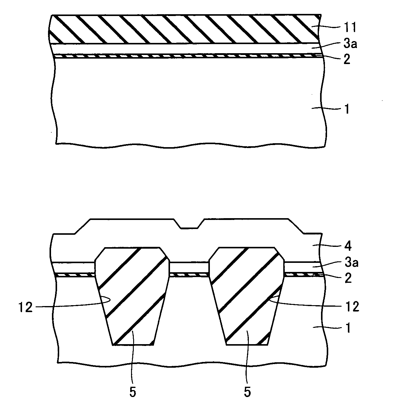
[0031]FIG. 1 is a cross section of the present nonvolatile memory device in a first embodiment as fabricated by SA-STI. In the figure, a semiconductor substrate 1 is provided with a plurality of element isolating insulation films (STIs) 5. Between STIs 5 is located an active region having a tunnel insulation film arranged thereon to form a gate insulation film 2. Furthermore on tunnel insulation film 2 a first silicon layer 3 and a second silicon layer 4 are deposited in layers to act as a floating gate, and thereon a control gate 13 is provided with an interlayer dielectric film 12 posed therebetween. Note that the first silicon layer 3 is located between two isolating insulation films 5 protruding above semiconductor substrate 1 and preferably has a thickness to have a height smaller than that of that portion of isolating insulation film 5 which protrudes.

[0032]FIG. 2 is a partially enlarged view of FIG. 1. In the present embodiment, as shown in FIG. 2, tunnel insulation film 2 c...

second embodiment

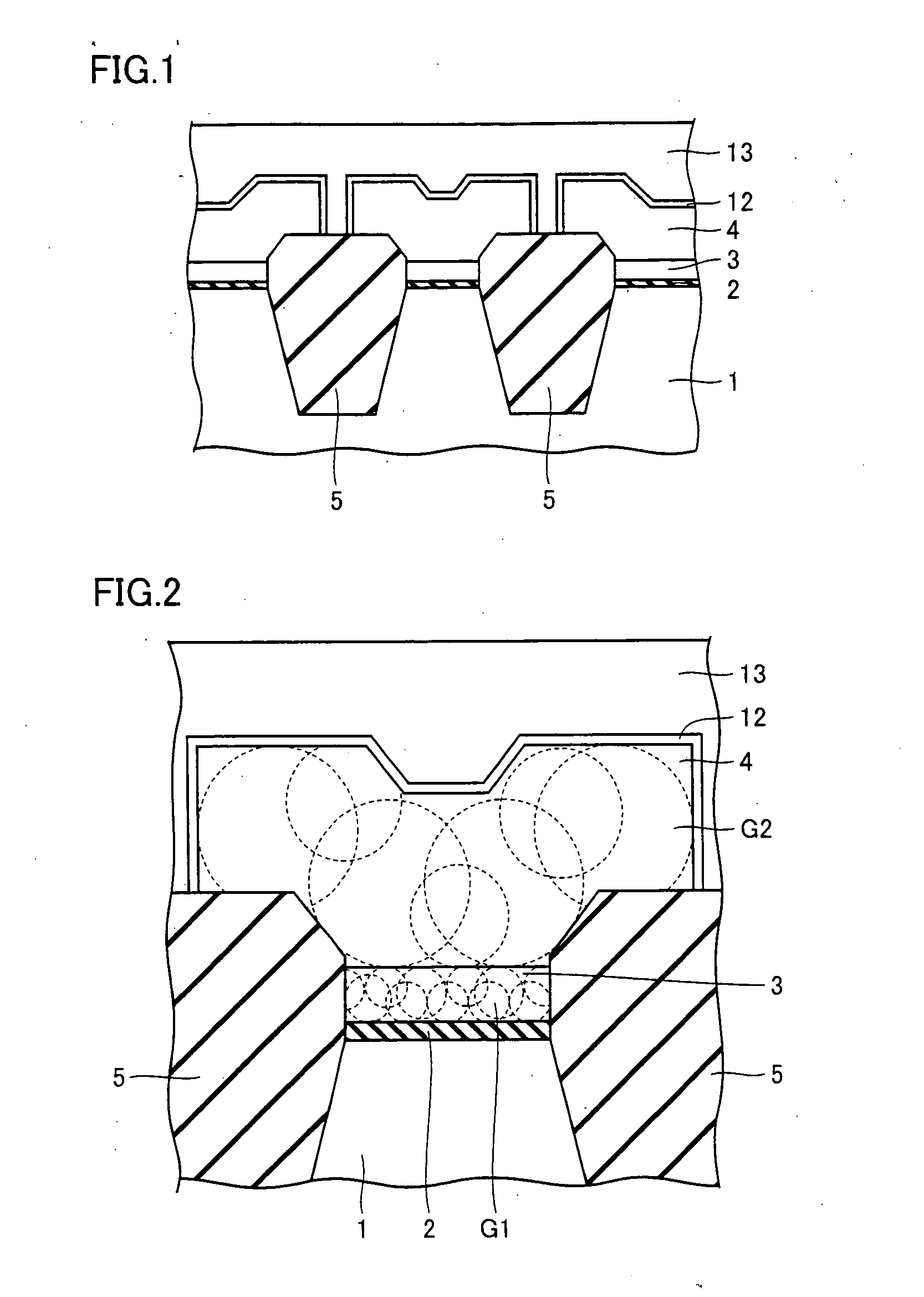
[0044] The present invention in a second embodiment is characterized in that the first polysilicon layer is increased in thickness and in addition thereto the first embodiment's satisfactory characteristic can be obtained. In the first embodiment a device structure, a method of fabrication and the like can require that the first silicon layer have a thickness of at least 50 nm. In that case, using amorphous silicon results in a crystal grain size increasing with film thickness and the present invention's object cannot be achieved. For such large film thickness, originally forming a polysilicon layer having a thickness in a range, as described hereinafter, allows as small a crystal grain size as approximately at most 30 nm.

[0045] More specifically, if the first polysilicon layer as originally deposited has a thickness set to be 50 to 70 nm, depositing the film at 600 to 650° C., preferably 620 to 630° C. allows the present invention's object to be achieved. Furthermore, if the first...


PUM


Abstract

A method includes the steps of: introducing insulation film into a trench to provide a trench isolation; planarizing the trench isolation to expose a passivation film; and removing the passivation film and depositing a second silicon layer on a first silicon layer and the trench isolation; and in the step of depositing the first silicon layer the first silicon layer is an undoped silicon layer and in the step of depositing the second silicon layer the second silicon layer is a doped silicon layer or an undoped silicon layer subsequently having an impurity introduced thereinto or the like and thermally diffused through subsequent thermal hysteresis into the first silicon layer.

Description

BACKGROUND OF THE INVENTION [0001] 1. Field of the Invention [0002] The present invention relates generally to semiconductor devices and methods of fabrication thereof and particularly to those utilizing self-aligned shallow trench isolation (SA-STI) for forming a gate electrode and an active region simultaneously. [0003] 2. Description of the Background Art [0004] For flash memory, self-aligned shallow trench isolation (SA-STI) has conventionally been employed. SA-STI allows a floating gate electrode's polysilicon and a shallow trench isolation (STI) to be formed with a single mask in self alignment. This technique has the following advantages: [0005] First, the STI is formed after a tunnel insulation film (or gate insulation film) is provided. This can prevent the tunnel insulation film from falling in at an end of an active region and thus thinning as typical STI would not avoid. As such, SA-STI can enhance the tunnel insulation film in reliability. [0006] Second, a trench and a ...

Claims


Application Information

Patent Timeline
Patent Type & Authority Applications(United States)
IPC IPC(8): H01L21/00H01L21/04H01L21/28H01L21/762H01L21/8247H01L27/115
CPCH01L21/28273H01L27/11521H01L27/115H01L21/76232H01L29/40114H10B69/00H10B41/30H01L21/76H10B99/00
Inventor MORINO, YASUKIKUSAKABE, YOSHIHIKOWAKAHARA, RYUICHI
Owner RENESAS TECH CORP
Why Eureka
Try Eureka