

Semiconductor device having a metal wiring structure and method of manufacturing the same
a technology of metal wiring and semiconductor devices, which is applied in the direction of semiconductor devices, semiconductor/solid-state device details, electrical equipment, etc., can solve the problems of reducing the effectiveness of the semiconductor device, reducing the contact resistance of the contact or the plug
- Summary
- Abstract
- Description
- Claims
- Application Information
AI Technical Summary
Benefits of technology
Problems solved by technology
Method used
Image

Examples
Embodiment Construction
[0043] The present invention now will be described more fully hereinafter with reference to the accompanying drawings, in which exemplary embodiments of the invention are shown. This invention may, however, be embodied in many different forms and should not be construed as limited to the embodiments set forth herein; rather, these embodiments are provided so that this disclosure will be thorough and complete, and will fully convey the scope of the invention to those skilled in the art. In the drawings, the thickness of layers and regions are exaggerated for clarity. Like reference numerals refer to similar or identical elements throughout. It will be understood that when an element such as a layer, region or wafer is referred to as being “on” or “onto” another element, it can be directly on the other element or intervening elements may also be present.
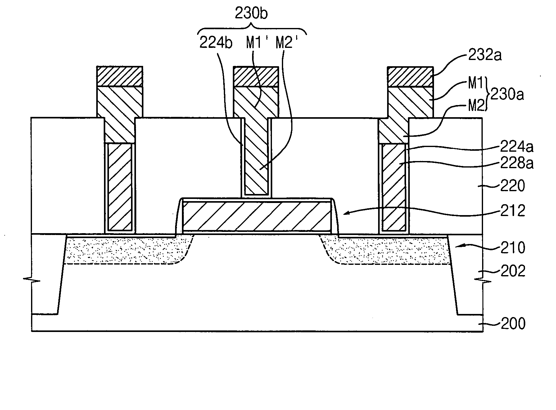
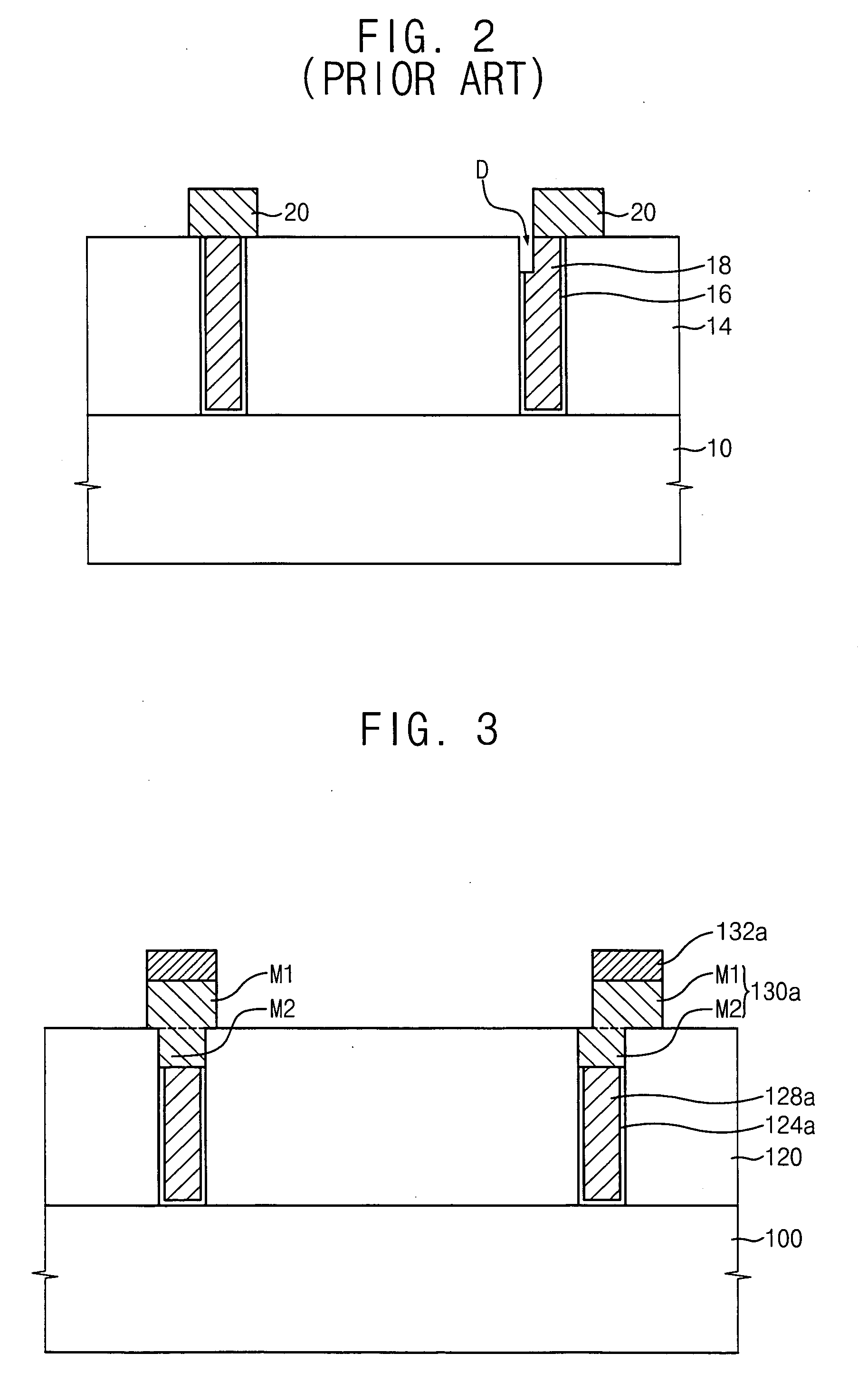
[0044]FIG. 3 is a cross sectional view illustrating a semiconductor device including a metal wiring structure and a plug in accordan...
PUM
 Abstract
Description
Claims
Application Information