Chip package substrate having soft circuit board and method for fabricating the same

a chip package and soft circuit board technology, applied in the direction of printed element electric connection formation, non-printed electric components of printed circuits, radio frequency controlled devices, etc., can solve the problems of reduced installation flexibility of the package body, increased material cost, high price of the ceramic package substrate, etc., to reduce manual operations, improve the yield of the product, and simplify the electric connection process

Inactive Publication Date: 2006-01-12
LITE ON SEMICON
View PDF3 Cites 5 Cited by
  • Summary
  • Abstract
  • Description
  • Claims
  • Application Information

AI Technical Summary

Benefits of technology

[0009] One object of the present invention is to provide a chip package substrate having a soft circuit board and a method for manufacturing the same, in which a package PCB and soft electric connection lines of an image-sensing chip are simultaneously finished for a single manufacturing process to simplify the electric connection process after chip packaging, reduce manual operations, and increase the yield thereof.
[0010] Another object of the present invention is to provide a chip package substrate having a soft circuit board, in which the size of the substrate and the soft electric connection lines are reduced to lower the cost.
[0011] Yet another object of the present invention is to provide a chip package substrate having a soft circuit board, in which soft electric connection lines are adhered on the chip package substrate with a larger area to enhance the adhesion strength and also increase the yield thereof
[0012] To achieve the above objects, the present invention provides a chip package substrate having a soft circuit board. The chip package substrate is used to package an image-sensing chip. The soft circuit board is used as external signal connection lines. The chip package substrate having a soft circuit board comprises a multi-layer soft and hard composite PCB, a plurality of conducting components and a plurality of conducting holes. The conducting holes are formed on the multi-layer soft and hard composite PCB. The conducting components are electroplated on the inner edges of the conducting holes on the multi-layer soft and hard composite PCB. An image-sensing chip can thus be packaged on the chip package substrate with the soft circuit board used as external signal connection lines to reduce the manufacturing cost and increase the yield thereof.

Problems solved by technology

Because the price of the ceramic package substrate is high, the material cost is thus increased.
Moreover, because it is necessary to connect the package body having the image-sensing chip firmly on the electronic board, the installation flexibility of the package body is thus reduced.
Because the comb-shaped electric connection sheet and the electric connection sheet of the hard PCB are glued together with conducting glue on a small area, the adhesion strength is low.
When the hard PCB and the soft circuit board having comb-shaped electric connection sheets are glued together, the comb-shaped electric connection sheet may be not completely pressed on the hard PCB due to unevenness of the end face of the hard PCB having the electric connection sheet, hence reducing the adhesion strength.
Moreover, it is necessary to use a microscope to view and align the adhesion portion of the two components, hence increasing the manufacturing time and wasting manpower.
Also, the conductivity of the conducting glue is reduced after a period of time at room temperature, hence lowering the yield.

Method used


Image

  • Chip package substrate having soft circuit board and method for fabricating the same
  • Chip package substrate having soft circuit board and method for fabricating the same
  • Chip package substrate having soft circuit board and method for fabricating the same

Examples


Embodiment Construction

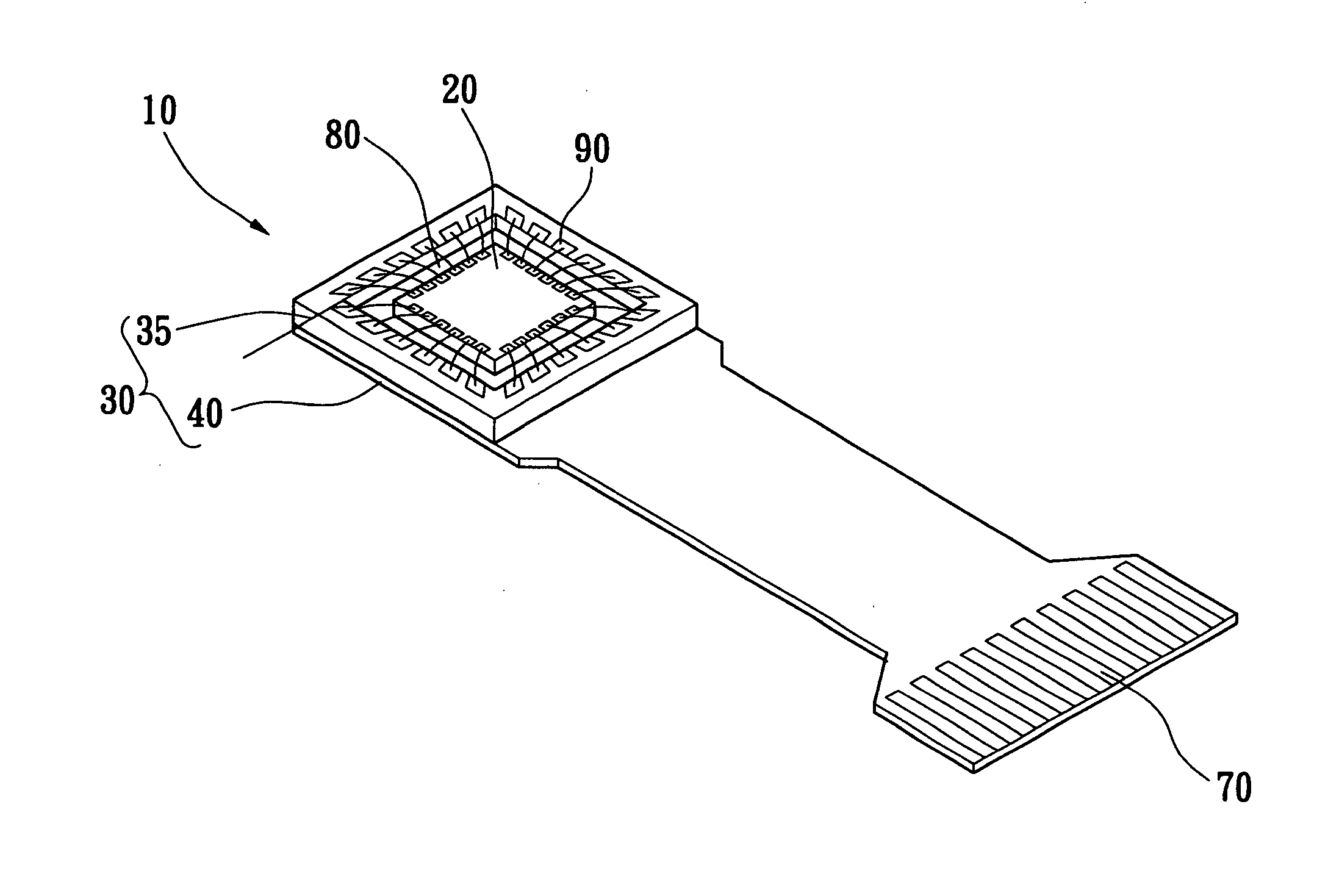
[0022] As shown in FIG. 3, the present invention provides a soft circuit board and a method for manufacturing the same. An image-sensing chip is packaged on the chip package substrate. The soft circuit board is used as external signal connection lines to connect an electronic board for forming an image detection module thereto. The method for manufacturing the chip package substrate having a soft circuit board provides manufacturing of the chip package substrate having a soft circuit board before chip packaging, hence simplifying the adhesion process of the soft circuit board after the chip is packaged on the chip package substrate.

[0023] As shown in FIGS. 3 and 4, a chip package substrate 10 having a soft circuit board is used to package an image-sensing chip 20. The soft circuit board is used as external signal connection lines. The chip package substrate 10 comprises a multi-layer soft and hard composite PCB 30, a plurality of conducting components 50 and a plurality of conducti...


PUM

PropertyMeasurementUnit
electricallyaaaaaaaaaa
transparentaaaaaaaaaa
flexibilityaaaaaaaaaa

Abstract

A chip package substrate having a soft circuit board jas a multi-layer soft and hard composite PCB, a plurality of conducting components and a plurality of conducting holes. The conducting holes are formed in the multi-layer soft and hard composite PCB. The conducting components are electroplated on the inner edges of the conducting holes on the multi-layer soft and hard composite PCB. An image-sensing chip can thus be packaged on the chip package substrate with the soft circuit board used as external signal connection lines, thereby saving the manufacturing cost and increasing the yield thereof.

Description

FIELD OF THE INVENTION [0001] The present invention relates to a chip package substrate having a soft circuit board and a method for manufacturing the same and, more particularly, to a chip package substrate with a soft circuit board formed on a soft and hard composite circuit board to be used as external signal connection lines. BACKGROUND OF THE INVENTION [0002] A common chip needs to be packaged and then electrically connected with an electronic board to be installed in an electronic device. In particular, an image-sensing chip needs to be protected by a package body and then electrically connected with an electronic board for operation. [0003]FIGS. 1A to 1G show the method for electrically connecting an image-sensing chip like a CCD or a CMOS sensor with an electronic board. First, a ceramic package substrate 10a is prepared. A groove 11a is formed in the upper side of the ceramic package substrate 10a. An image-sensing chip 20a is then adhered in the groove 11a of the ceramic p...

Claims


Application Information

Patent Timeline
Patent Type & Authority Applications(United States)
IPC IPC(8): H01L31/0203H01L21/00H01L23/12H01L27/146H05K1/18H05K3/00H05K3/42
CPCH01L27/14618Y10T29/49155H05K1/183H05K1/189H05K3/0052H05K3/42H05K3/4691H05K2201/09036H05K2201/0949H05K2203/049Y10T29/49165Y10T29/49126Y10T29/49121Y10T29/49117H01L31/0203H01L2224/05554H01L2224/48091H01L2224/49171H01L2924/00014
Inventor CHEN, HUEI-JENLIU, EVANCHEN, YVON
Owner LITE ON SEMICON
Why Eureka
Try Eureka