Structure of a micro electro mechanical system

a micro-electromagnetic system and structure technology, applied in the field of micro-electromagnetic system, can solve the problems of increasing process difficulty, narrow viewing angle of thin film transistor liquid crystal display, and complicated process steps in the above-mentioned method, so as to simplify the composition structure of reflective display units and reduce the effect of light leakag

Inactive Publication Date: 2006-01-12
SNAPTRACK
View PDF98 Cites 178 Cited by
  • Summary
  • Abstract
  • Description
  • Claims
  • Application Information

AI Technical Summary

Benefits of technology

[0010] Still another objective of the present invention is to provide a micro electro mechanical system to be used as a reflective display unit, which is set in front of the reflective elements to shield the reflective elements and controls the reflection of incident light and the amount of reflected incident light to control further different reflective display units to produce gray scales.
[0021] Since the reflective display units provided by the present invention are not restricted to the usage of the polarized light as conventional liquid crystal molecules are, there is no restriction in view angle. Further, the micro electro mechanical system provided by the present invention does not need to use the polarized light produced from the two polarizers above or below the liquid crystal molecule as the conventional liquid crystal molecule does, so polarizers are not needed above or below, and the efficiency of the usage of light is greatly increased.

Problems solved by technology

However, since the conventional liquid crystal display uses polarized light to twist the crystal molecule, the view angle of the thin film transistor liquid crystal display is narrow.
However, the process steps in the aforementioned method are complicated.
The difficulty of process is thus increased.
However, the step is time-consuming, and thus cannot achieve a fast response.
If the liquid crystal molecule is used as the switch to control the penetration of the light, it is hard to avoid the aforementioned problem.

Method used


Image

  • Structure of a micro electro mechanical system
  • Structure of a micro electro mechanical system
  • Structure of a micro electro mechanical system

Examples


embodiment 1

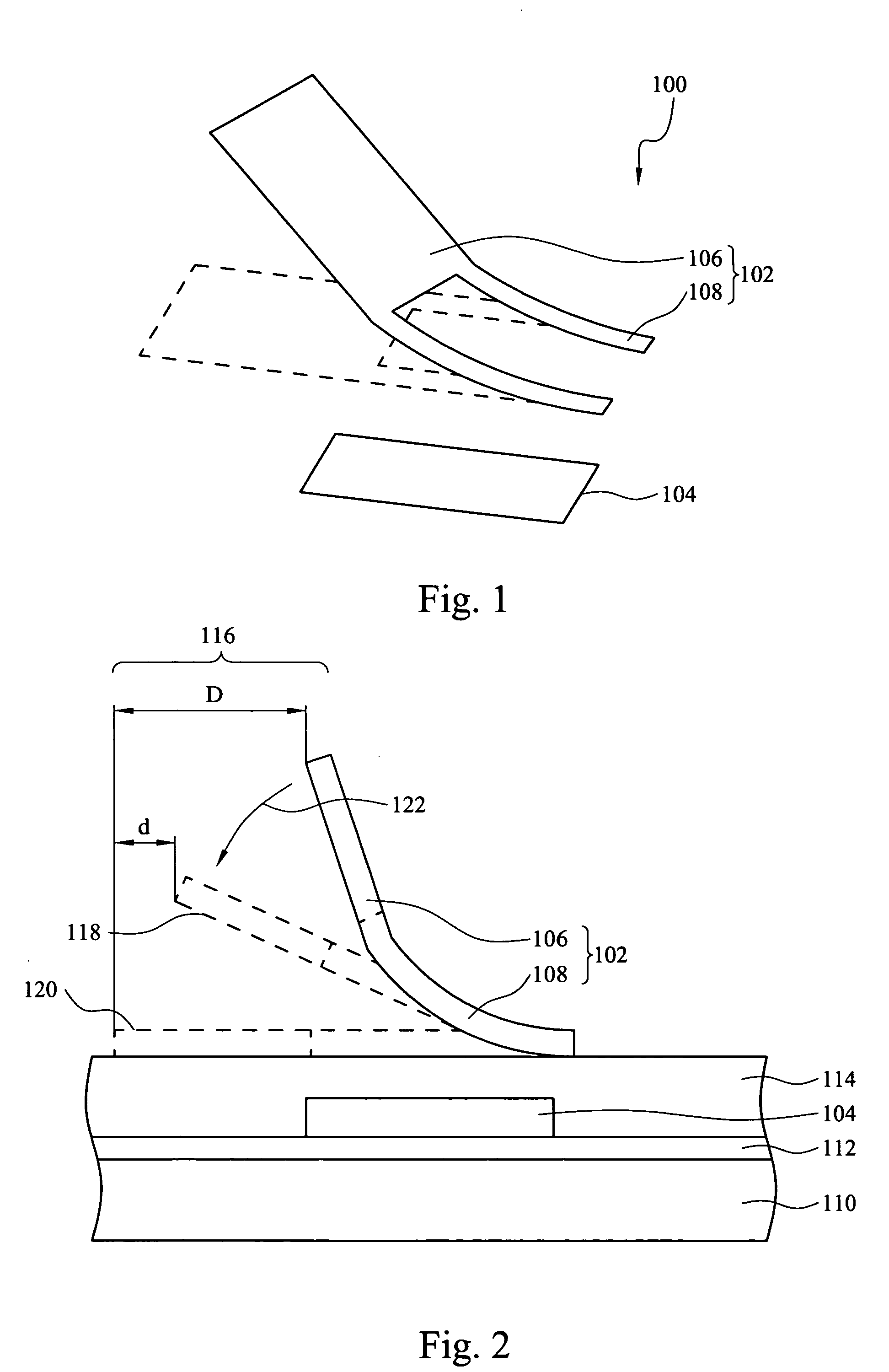
[0030] Reference is made to FIG. 1, which is a three-dimensional diagram of the display unit of a micro electro mechanical system provided by the present invention. The display unit of a micro electro mechanical system 100 includes an upper electrode 102 and a lower electrode 104, in which the upper electrode 102 and the lower electrode 104 are located on a transparent substrate (not shown in the drawing). The upper electrode 102 is composed of two kinds of material having different stress. One is a low stress structure 106 used as a shielding electrode, and the other is a high stress structure 108 connecting to one side of the low stress structure 106. The high stress structure 108 drives the low stress structure 106 to rotate along a substantial or virtual axis (not shown in the drawing). This will affect the shielding effect of the light source below the lower electrode 104 (not shown in the drawing) to different extents. The lower electrode 104 is located below the high stress s...

embodiment 2

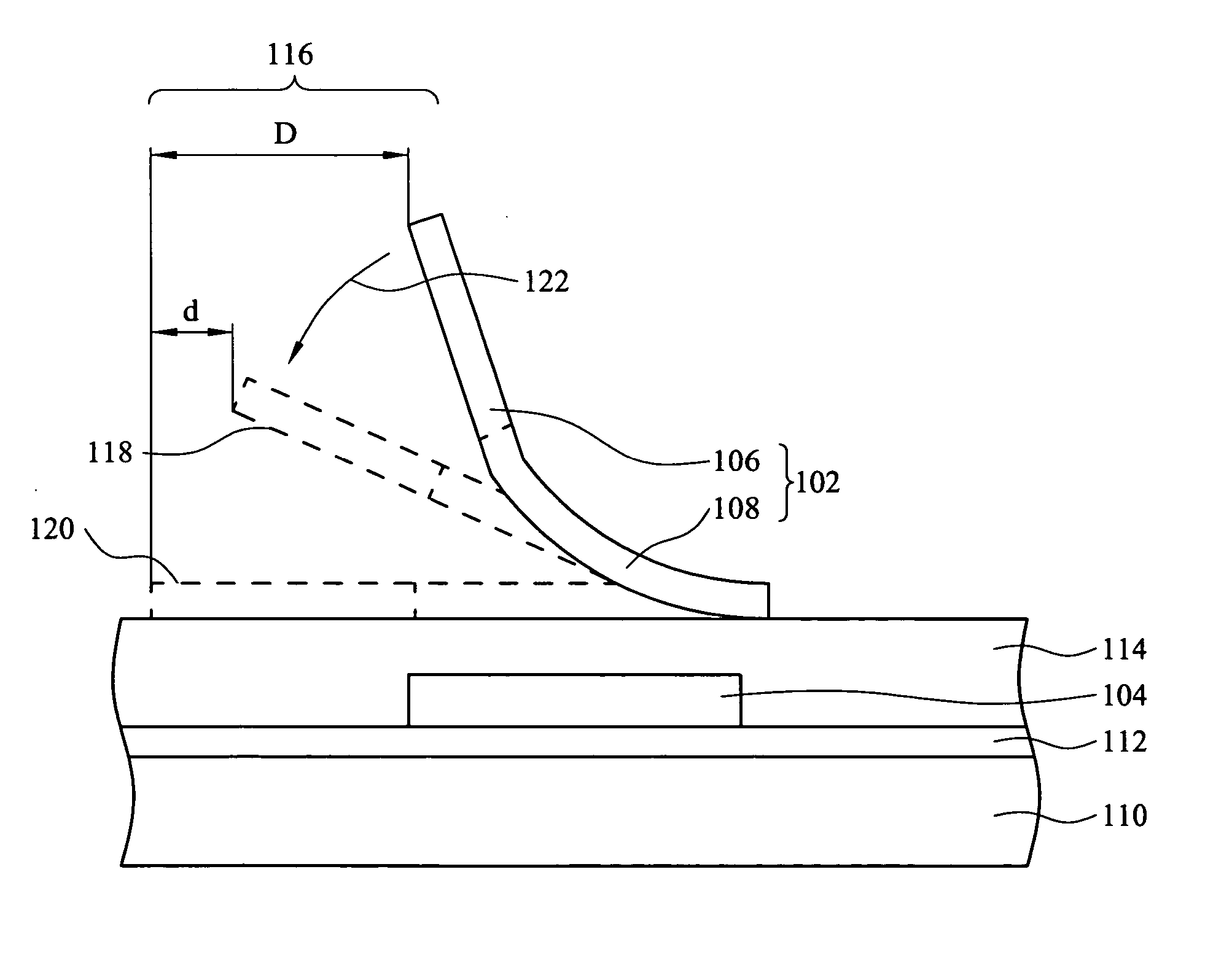
[0031] Reference is made to FIG. 2, which is a cross-sectional diagram of the display unit of a micro electro mechanical system provided by the present invention. A lower electrode 104 is located on a transparent substrate 110. At least a dielectric layer 112 is located between the lower electrode 104 and the transparent substrate 110. A dielectric layer 114 is located on the lower electrode 104 as an insulating layer. A light-penetrating area 116 is located on the left side of the lower electrode 104. When used in transmissible display units, the light from the light source below the transparent substrate 110 (not shown in the drawing) penetrates through the area and is seen by viewers.

[0032] An upper electrode 102 is located on the dielectric layer 114. The upper electrode 102 comprises a low stress structure 106 and a high stress structure 108, in which the high stress structure 108 is connected to one side of the low stress structure 106. The high stress structure 108 is locate...

embodiment 3

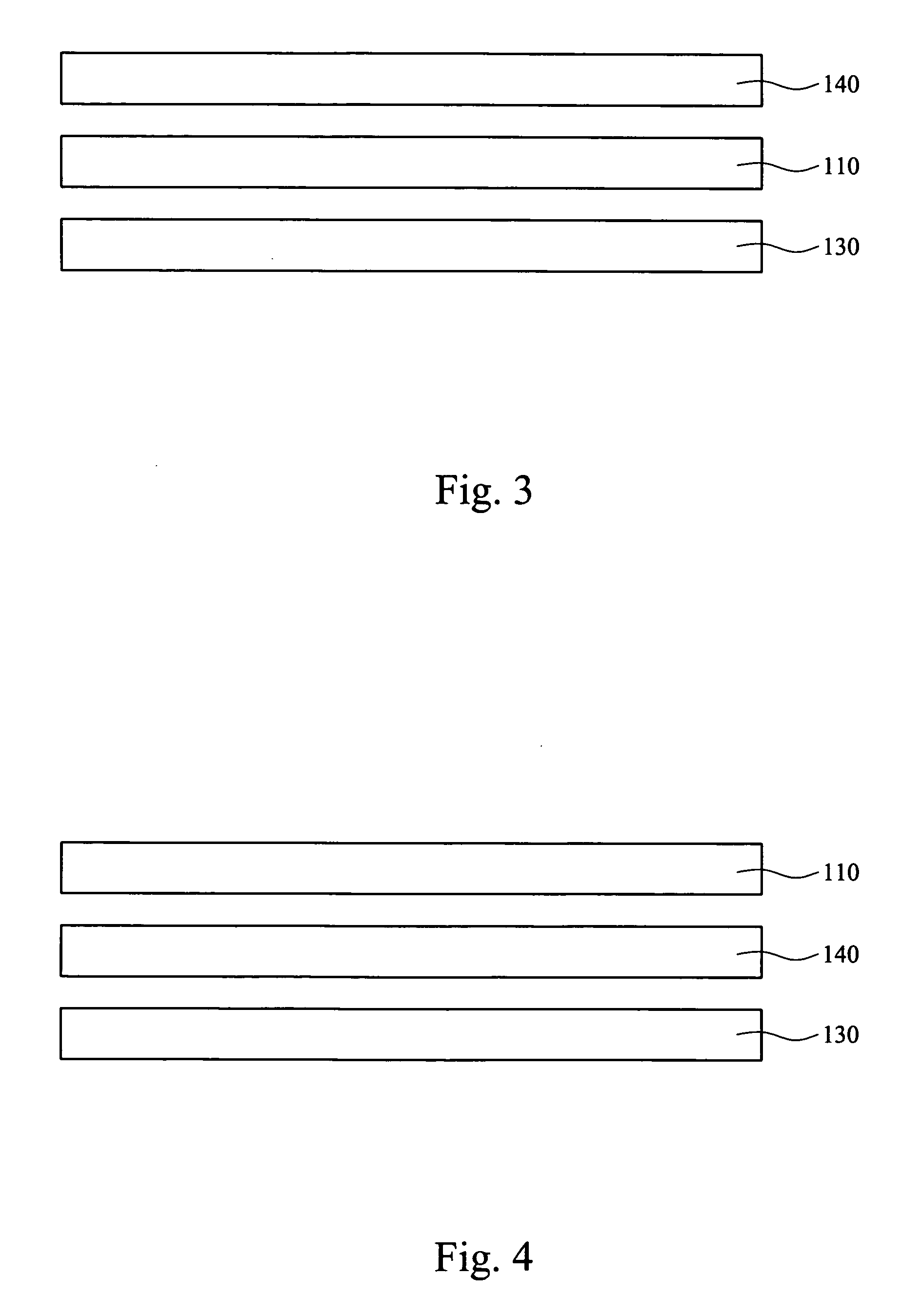
[0035] Reference is made to FIG. 3 illustrating the application of transmissible display units disclosed by the present invention on a multicolor planar display apparatus. A transparent substrate 110 having transmissible display units is put between a back light source 130 and a color filter 140. The transparent substrate 110 having transmissible display units can replace conventional liquid crystal molecules and serve as a switch to control the light penetrating through the planar display apparatus. FIG. 4 illustrates another embodiment of the application of transmissible display units disclosed by the present invention on a multicolor planar display apparatus. The color filter 140 is placed between the transparent substrate 110 having transmissible display units and the back light source 130. The transparent substrate 110 having transmissible display units can still replace conventional liquid crystal molecules and serve as a switch to control the light penetrating through the pla...


PUM

PropertyMeasurementUnit
voltageaaaaaaaaaa
stressaaaaaaaaaa
transparentaaaaaaaaaa

Abstract

A structure of a micro electro mechanical system (MEMS) for a planar display apparatus is described. The MEMS structure used as a transmissible or reflective display device has a shielding electrode and a control electrode. The shielding electrode has a low stress electrode and a high stress electrode. The high stress electrode connected to the low stress electrode is a movable element. The control electrode is located below the high stress electrode. The control electrode attracts the high stress electrode when a voltage is applied to the control electrode. The high stress electrode deforms and the position of the low stress electrode is altered.

Description

RELATED APPLICATIONS [0001] The present application is based on, and claims priority from, Taiwan Application Serial Number 93120662, filed Jul. 9, 2004, the disclosure of which is hereby incorporated by reference herein in its entirety. FIELD OF THE INVENTION [0002] The present invention relates to a micro electro mechanical system for a transmissible or reflective display unit structure, and more particularly, to a transmissible or reflective display unit structure suitable for use in a planar display apparatus. BACKGROUND OF THE INVENTION [0003] Since a planar display apparatus is small and lightweight, it has predominance in the portable display device and small-volume display markets. At present, the mainstream planar display apparatus is the liquid crystal display (LCD). [0004] Most liquid crystal displays at present turn each crystal molecule on and off by the twisting and rearranging of the crystal molecules in the electric field. However, since the conventional liquid cryst...

Claims


Application Information

Patent Timeline
Patent Type & Authority Applications(United States)
IPC IPC(8): G02F1/03B81B7/02G02B26/02G02F1/01
CPCG02B26/02G02F1/1335
Inventor TSAI, HSIUNG-KUANG
Owner SNAPTRACK
Why Eureka
Try Eureka