Dual polarity, high input voltage swing comparator using MOS input transistors

a technology of input transistor and comparator, which is applied in the direction of pulse circuit, instant pulse delivery arrangement, pulse technique, etc., can solve the problems of input voltage limitations and limitations, and achieve high input impedance, high input impedance, and high input voltage swing

Active Publication Date: 2006-01-19
TEXAS INSTR INC
View PDF14 Cites 22 Cited by
  • Summary
  • Abstract
  • Description
  • Claims
  • Application Information

AI Technical Summary

Benefits of technology

[0005] The present invention achieves technical advantages as a differential input comparator using MOS input transistors, for dual polarity high input voltage swing applications and high input impedance.
[0006] In one embodiment, a differential input comparator circuit comprises an input stage comprising dual polarity input voltages and an output stage adapted to output a differential voltage based on the input voltages, wherein the differential voltage is adapted to be transmitted to a comparator and wherein the circuit has high input impedance and works with high input voltage swings.
[0007] In another embodiment, a method for comparing signals comprises receiving dual polarity input voltages, maintaining a high input impedance, converting the dual polarity input voltages to a single polarity output voltage and outputting the single polarity output voltage, based on the input voltages, to a comparator.

Problems solved by technology

Various problems are associated with comparator circuits, in particular with the input stage of the comparator.
For example, input voltage limitations exist.
Such limitations are imposed by the voltage breakdown of PN junctions and gate oxides in an ordinary complementary MOS (CMOS) or bipolar CMOS (BiCMOS) fabrication process.

Method used


Image

  • Dual polarity, high input voltage swing comparator using MOS input transistors
  • Dual polarity, high input voltage swing comparator using MOS input transistors
  • Dual polarity, high input voltage swing comparator using MOS input transistors

Examples


Embodiment Construction

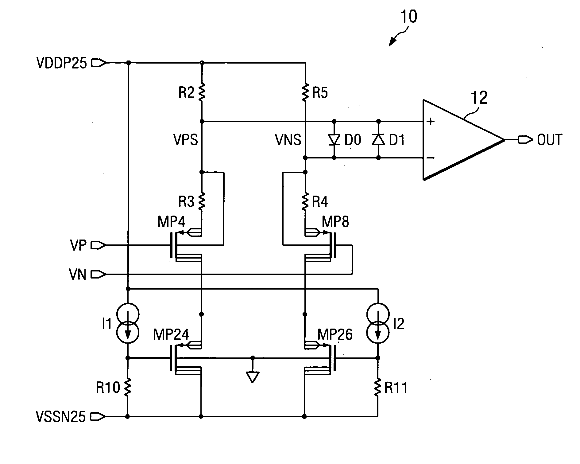
[0022] Referring now to FIG. 1a, a differential input comparator circuit 10 of the present invention includes an input stage that comprises positive Channel MOS (PMOS) transistors MP4, MP8, MP24, and MP26, resistors R2, R3, R4, R5, R10, and R11, diodes D0 and D1, current sources I1 and I2 voltage supplies VDDP25 and VSSN25, and a circuit ground node gnd. The output of this first stage is the differential voltage VPS-VNS which is applied to an ordinary comparator 12. Comparator 12 works only with single positive polarity signals so the first stage converts the dual polarity signals applied to VP and VN to positive voltages at VPS and VNS.

[0023] Resistor R2 is connected between supply voltage VDDP25 and the common node VPS of R2, R3, D0, D1, the N-well of transistor MP4, and the positive input of comparator 12. Resistor R3 is connected between the common node VPS and the source of PMOS transistor MP4. The gate of transistor MP4 is connected to differential input signal voltage VP. Th...


PUM


Abstract

A differential input comparator circuit comprises an input stage comprising dual polarity input voltages and an output stage adapted to output a differential voltage based on the input voltages, wherein the differential voltage is adapted to be transmitted to a comparator and wherein the circuit has high input impedance and works with high input voltage swings.

Description

FIELD OF THE INVENTION [0001] The present invention relates to differential input comparators and, more particularly, to a differential input comparator using MOS input transistors, for dual polarity, high voltage swing applications. BACKGROUND OF THE INVENTION [0002] A comparator circuit typically receives two input signals and generates an output signal based on the comparison of the two input signals. The comparison is generally based on the amplitude or magnitude of the input voltages. [0003] Various problems are associated with comparator circuits, in particular with the input stage of the comparator. For example, input voltage limitations exist. Such limitations are imposed by the voltage breakdown of PN junctions and gate oxides in an ordinary complementary MOS (CMOS) or bipolar CMOS (BiCMOS) fabrication process. Further, certain solutions to these problems associated with comparator circuits employ external components to the chip or make use of circuit configurations that lo...

Claims


Application Information

Patent Timeline
Patent Type & Authority Applications(United States)
IPC IPC(8): H03K5/153
CPCH03K5/2481
Inventor MARTINS, MARCUS MARCHESI
Owner TEXAS INSTR INC
Why Eureka
Try Eureka