Display device and electronic apparatus using the same
a technology of electronic equipment and display device, which is applied in the field of display device, can solve the problems of reducing reliability as a mobile device, increasing the size and weight of the device, and unable to accurately perform luminance control
- Summary
- Abstract
- Description
- Claims
- Application Information
AI Technical Summary
Benefits of technology
Problems solved by technology
Method used
Image
Examples
embodiment 1
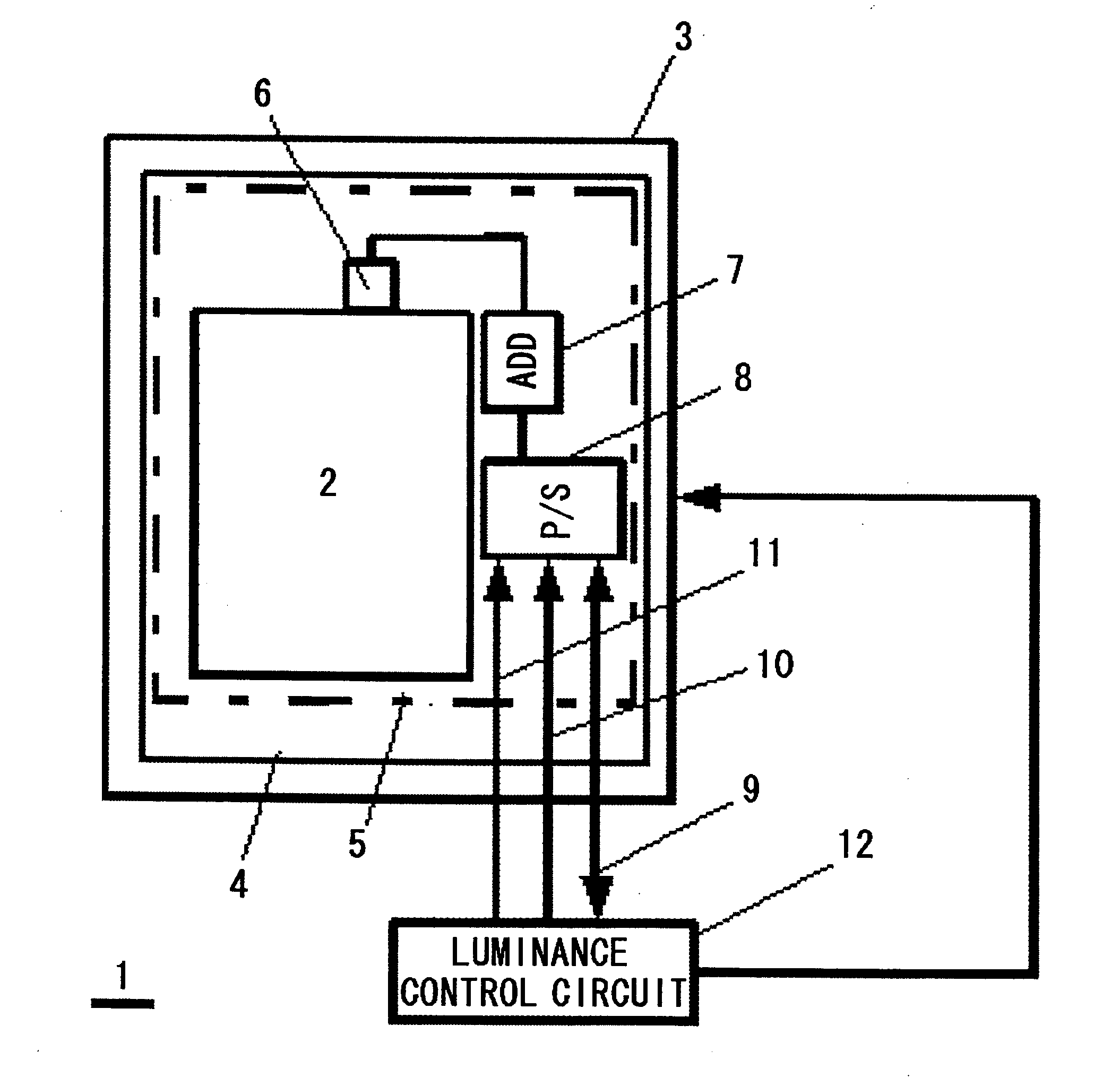
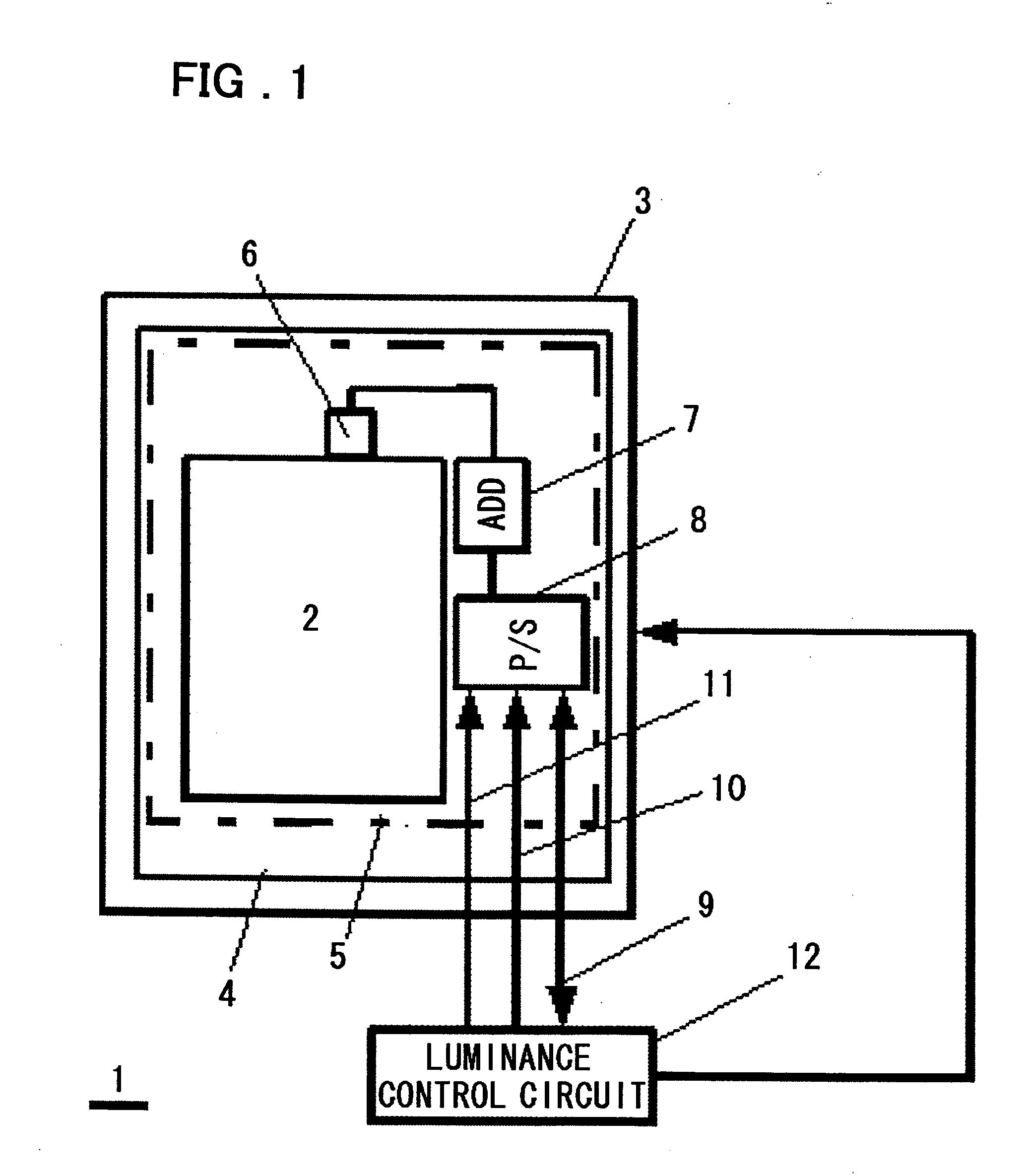
[0028] Next, a first preferred embodiment in which the present invention is applied to a transmission-type LCD with a backlight using an LED (Light Emitting Diode) will be described. The display device 1 relating to the present embodiment comprises an optical sensor 6, analog-to-digital converter circuit (ADC hereinafter) 7, and a serial-parallel converter circuit 8 provided on a substrate 4 on which a TFT driving pixels is provided, converts an output signal of the sensor 6 into a digital signal, and enables the digital signal converted into serial data to be transmitted to use it for the luminance control of the display device, corresponding to external chip-select signals.
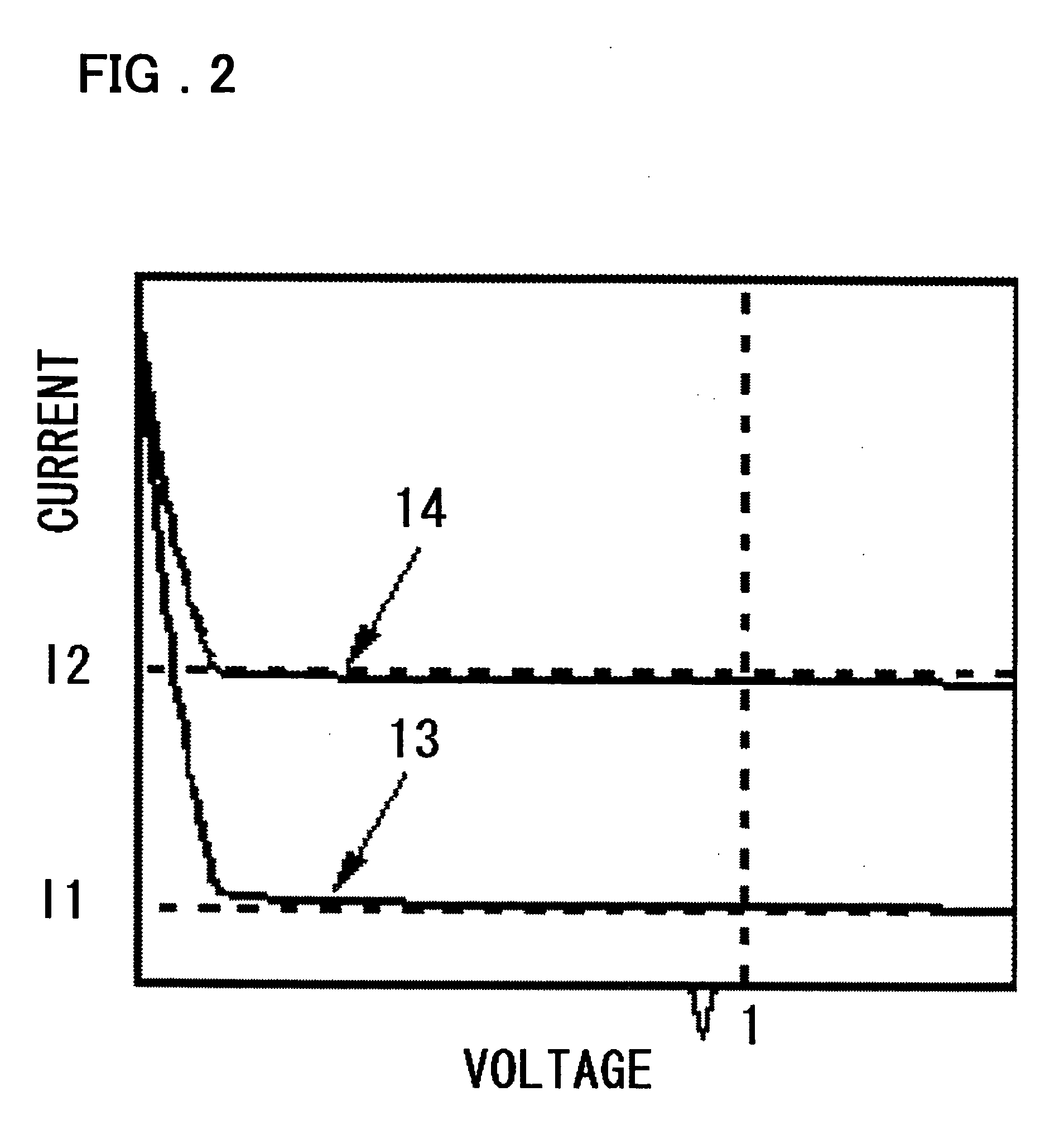
[0029]FIG. 1 is an outline drawing of the display device relating to the first embodiment of the present invention. In reference to FIG. 1, the display device 1 comprises a backlight 3, which is the light source, the TFT substrate 4, on which the pixels (electrodes) and the TFT driving liquid crystal are provid...
embodiment 2
[0045] Next, a second embodiment in which the present invention is applied to a transmission-type LCD, as in the first embodiment, will be described. FIG. 4 is an outline drawing of the display device relating to the second embodiment of the present invention. In reference to FIG. 4, the display device 1 comprises a backlight 3, a TFT substrate 4, on which pixels (electrodes) and a TFT driving liquid crystal are provided, and a counter substrate 5 disposed so that a liquid crystal layer, not shown in the drawing, is interposed between the TFT substrate 4 and the counter substrate 5, and a display region 2 is provided.
[0046] On the TFT substrate 4, an optical sensor 6 using a photodiode is formed using the means described in Japanese Patent Kokai Publication No. JP-A-06-11690 or the like. Similarly, a luminance control circuit 15 that controls the luminance of the backlight 3 based on a signal from the optical sensor 6 is formed on the top of the TFT substrate 4. Here, the optical s...
embodiment 3
[0053] Next, a third embodiment in which the present invention is applied to a transmission-type LCD, as in the first and second embodiments, will be described. FIG. 7 is an oblique perspective drawing showing the outline structure of the display device relating to the third embodiment of the present invention. In reference to FIG. 7, the display device 1 comprises a backlight 3, a TFT substrate 4, on which pixels (electrodes) and a TFT driving liquid crystal are provided, a counter substrate 5 disposed so that a liquid crystal layer, not shown in the drawing, is interposed between the TFT substrate 4 and the counter substrate 5, and a luminance control circuit 24, and a display region 2 is provided.
[0054] On the TFT substrate 4, an optical sensor 6 using a photodiode and a thin film wiring 19 are formed using the means described in Japanese Patent Kokai Publication No. JP-A-06-11690 or the like. Similarly, utilizing the COG (chip-on-glass) process, an IC 20 that includes an ADC an...
PUM
 Abstract
Description
Claims
Application Information
 - R&D
- Intellectual Property
- Life Sciences
- Materials
- Tech Scout
- Unparalleled Data Quality
- Higher Quality Content
- 60% Fewer Hallucinations
Browse by: Latest US Patents, China's latest patents, Technical Efficacy Thesaurus, Application Domain, Technology Topic, Popular Technical Reports.
© 2025 PatSnap. All rights reserved.Legal|Privacy policy|Modern Slavery Act Transparency Statement|Sitemap|About US| Contact US: help@patsnap.com


