Data processing method, data processing apparatus, semiconductor device, and electronic apparatus

a data processing apparatus and data processing technology, applied in the field of data processing methods, data processing apparatuses, semiconductor devices, electronic devices, etc., can solve the problems of insufficient combination of ad conversion and computation processing, insufficient mechanism for performing addition/subtraction of signals in an analog area and digitizing the resulting signals,

Inactive Publication Date: 2006-01-19
SONY CORP
View PDF4 Cites 73 Cited by
  • Summary
  • Abstract
  • Description
  • Claims
  • Application Information

AI Technical Summary

Problems solved by technology

However, in the above-described known mechanisms, a combination of the AD conversion and computation processing is not sufficient since it has advantages and disadvantages in terms of both the processing and the circuit arrangement.
For example, the mechanism for performing addition / subtraction on signals in an analog area and then digitizing the resulting signals is not always efficient.

Method used


Image

  • Data processing method, data processing apparatus, semiconductor device, and electronic apparatus
  • Data processing method, data processing apparatus, semiconductor device, and electronic apparatus
  • Data processing method, data processing apparatus, semiconductor device, and electronic apparatus

Examples


first embodiment

Spatial Difference Processing Operation

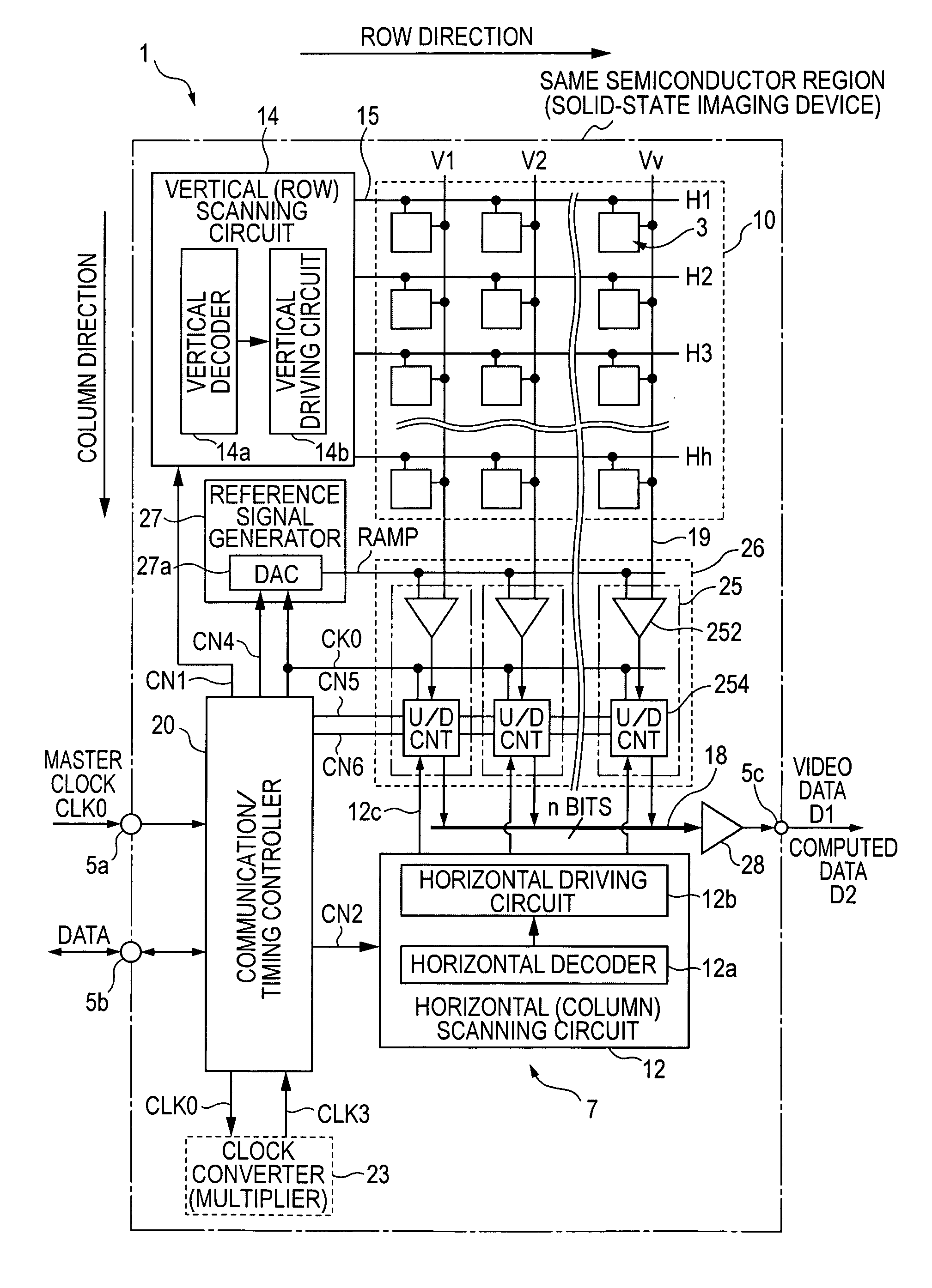
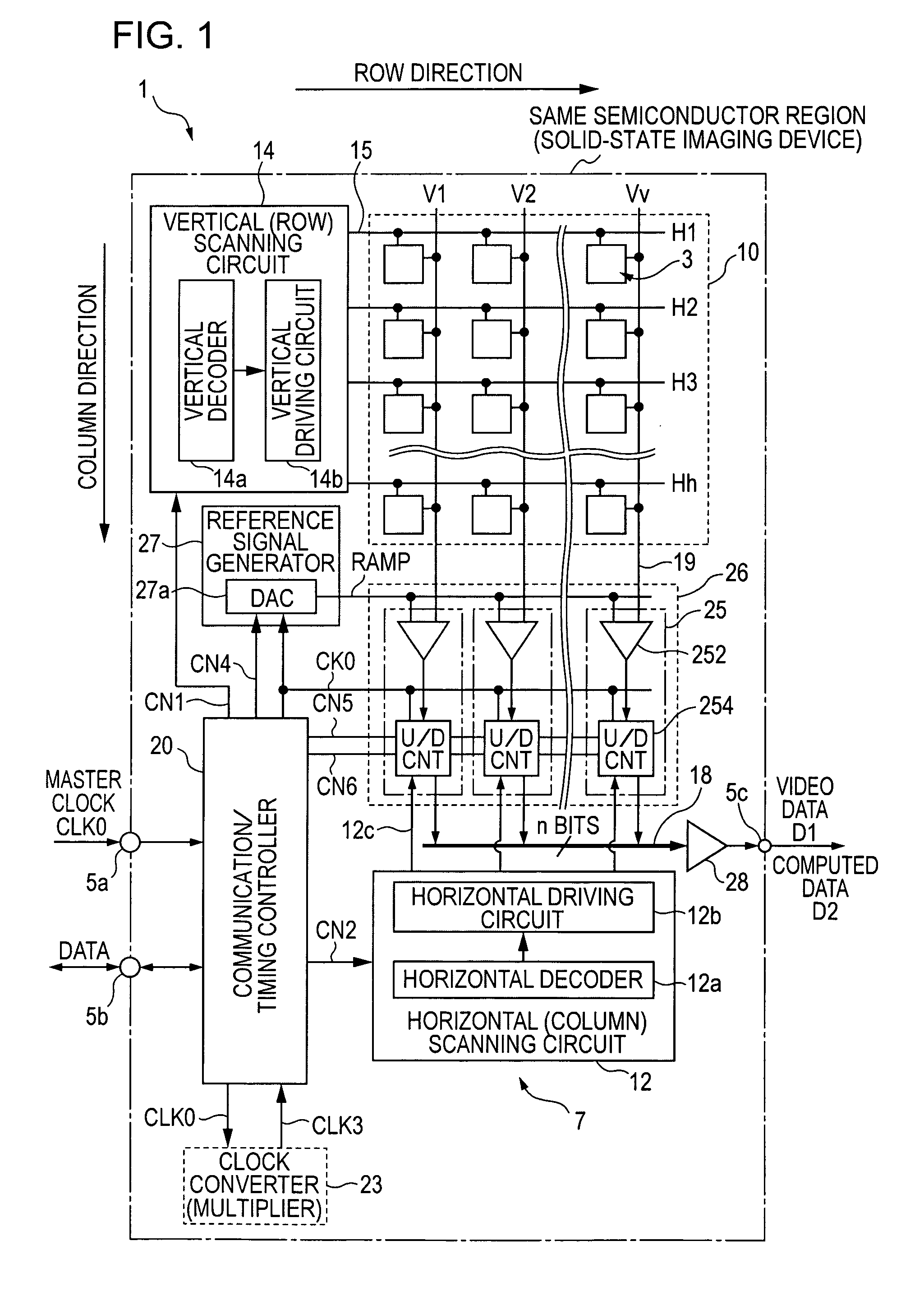
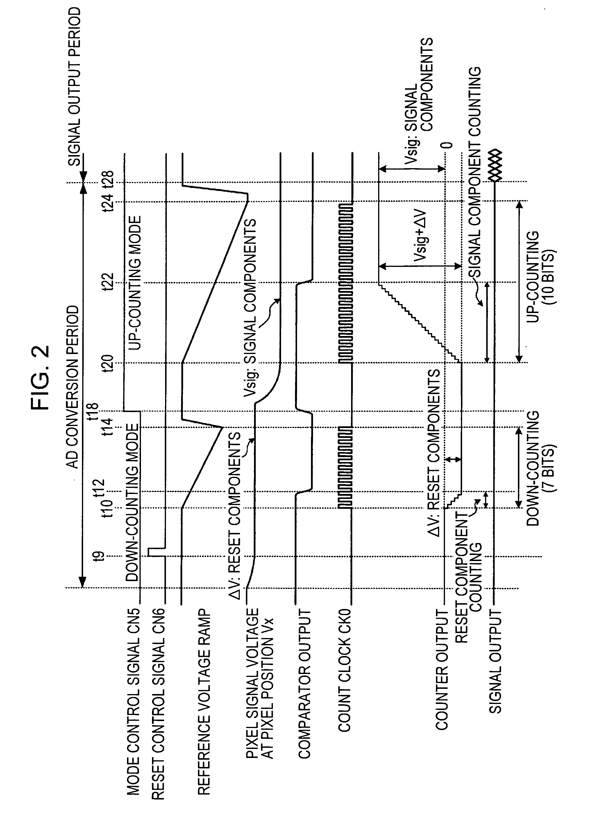
[0157]FIG. 3 is a timing chart illustrating the operation of the spatial difference processing operation in the column AD circuit 25 of the solid-state imaging device 1 of the second embodiment shown in FIG. 1. The spatial difference processing is difference processing between a plurality of pixel signals located at different pixel positions in one field of an image which is captured substantially at the same time.

[0158] The reason for describing the “captured substantially at the same time” is due to the circumstance unique to the CMOS sensors where the charge accumulation period is different by horizontal lines because scanning is performed in each horizontal line (scanning line). By the use of, for example, a mechanical shutter, or by adding a global exposure function to the CMOS sensor, all the horizontal lines have the same charge accumulation period so that one field of an image can be captured exactly at the same time.

[0159] Typical e...

second embodiment

Spatial Difference Processing Operation by Solid-State Imaging Device

[0184]FIG. 6 is a timing chart illustrating the operation of the spatial difference processing operation in the column AD circuit 25 of the solid-state imaging device 1 of the second embodiment shown in FIG. 4.

[0185] In the second embodiment, as shown in FIG. 5, since the count value indicating the previous subtraction processing result is transferred to the data storage unit 256 before the first readout operation (AD conversion) for the pixel signal to be processed, the readout operation is not restricted.

[0186] With this arrangement, as shown in FIG. 6, the signal output operation for outputting the difference data to the outside the imaging apparatus 1 from the data storage unit 256 via the horizontal signal line 18 and the output circuit 28 can be simultaneously performed with the difference operation utilizing the readout operation for reading the signals in the current row Hx and the subsequent row (Hx+1) ...

third embodiment

Spatial Difference Processing Operation of Solid-State Imaging Device

Two-Dimensional Processing


PUM


Abstract

In a solid-state imaging device with an AD converter mounted on the same chip, to enable an efficient product-sum operation while reducing the size of the circuit scale and the number of transmission signal lines. A pixel signal during an n-row readout period is compared with a reference signal for digitizing this pixel signal, and a counting operation is performed in one of a down-counting mode and an up-counting mode while the comparison processing is being performed, and then, the count value when the comparison processing is finished is stored. Subsequently, by using the n-row counting result as the initial value, a pixel signal during an (n+1)-row readout period is compared with the reference signal for digitizing this pixel signal, and also, the counting operation is performed in one of the down-counting mode and the up-counting mode, and then, the count value when the comparison processing is finished is stored. If the count mode for the n+1 row is set to be opposite to the count mode for the n row, the count value obtained by the counting operation for the n+1 row is a subtraction result. If the count modes for the n+1 row and the n row are set to be the same, the count value obtained by the counting operation for the n+1 row is an addition result

Description

CROSS PREFERENCE TO RELATED APPLICATIONS [0001] The present invention claims the benefit of Japanese Patent Application JP 2004-209886 filed in the Japanese Patent Office on Jul. 16, 2004, the entire contents of which are incorporated herein by reference. FIELD OF THE INVENTION [0002] The present invention relates to a data processing method, a data processing apparatus, a semiconductor device for detecting the physical quantity distribution in which a plurality of unit elements are disposed, and an electronic apparatus, for instance, a camera. More specifically, the invention relates to a digital signal processing technology suitably used for semiconductor devices for detecting the physical quantity distribution, for example, solid-state imaging devices, and other electronic apparatuses, in which a plurality of unit elements responsive to electromagnetic waves, such as light or radiation, input from an external source, are disposed, and the physical quantity distribution obtained b...

Claims


Application Information

Patent Timeline
Patent Type & Authority Applications(United States)
IPC IPC(8): G06K9/46G06V10/20H03M1/56H04N5/335H04N5/374H04N5/378H04N9/07
CPCG06K9/60H04N5/37455H04N5/367H04N3/155G06V10/20H04N25/68H04N25/75
Inventor NITTA, YOSHIKAZUFUKUSHIMA, NORIYUKIMURAMATSU, YOSHINORIYASUI, YUKIHIRO
Owner SONY CORP
Why Eureka
Try Eureka