Device for identifying types of sheet materials
a sheet material and identification technology, applied in the direction of electrographic process, optical radiation measurement, instruments, etc., can solve the problems of inability to detect the water content, inability to detect accurate sheet material information, limited information that sheet materials can carry, etc., to achieve the effect of detecting accurate information of sheet materials
- Summary
- Abstract
- Description
- Claims
- Application Information
AI Technical Summary
Benefits of technology
Problems solved by technology
Method used
Image
Examples
example 1
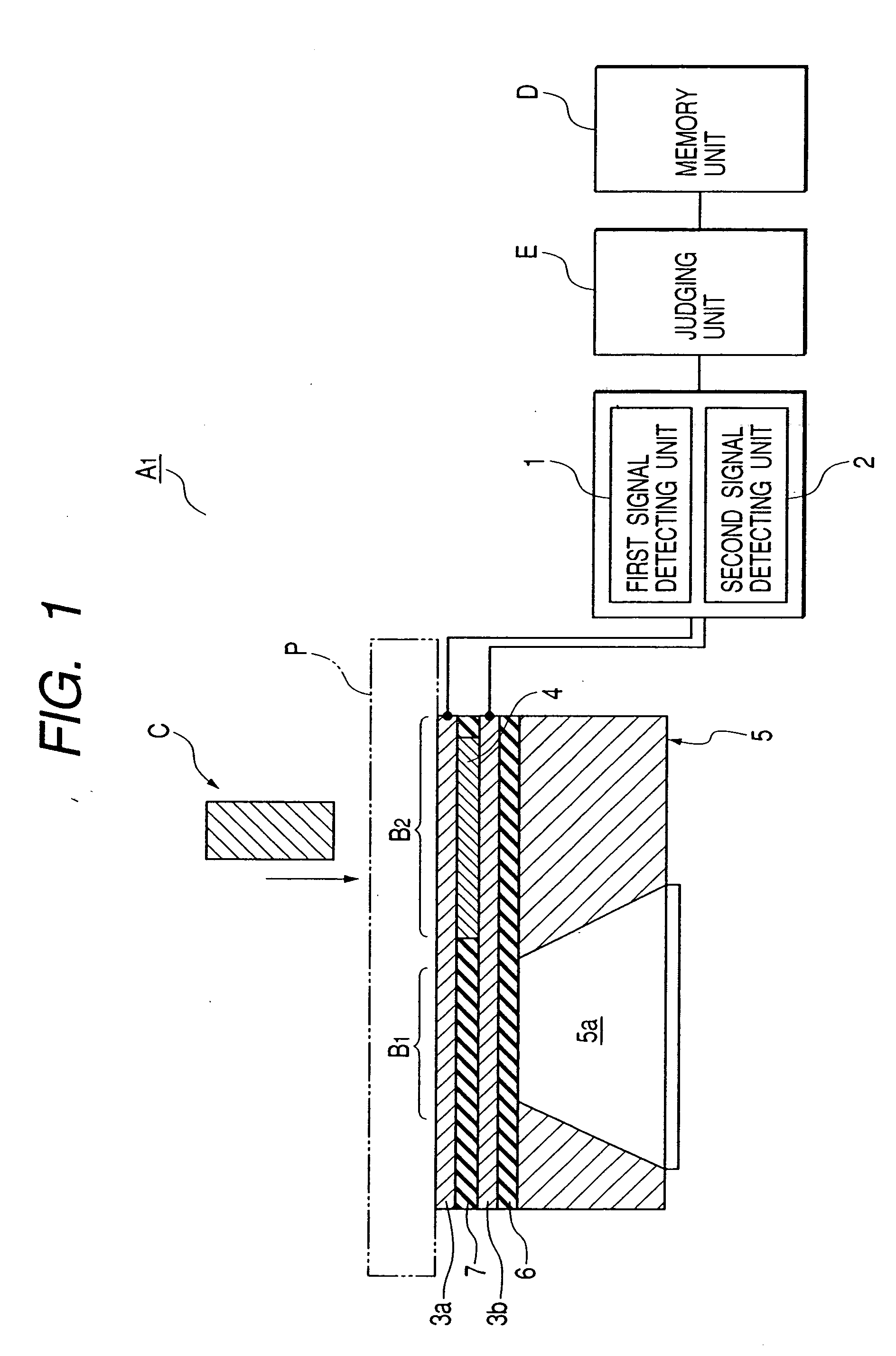
[0075] In this example, a sheet identifying device (information detecting device) having a structure as shown in FIG. 1 was manufactured.
[0076] The metal oxide 4 was formed from PbZrTiO3 (Zr / Ti=35 / 65) (hereinafter abbreviated as PZT) and Pt was used for the electroconductive members 3a and 3b. To improve the adhesion between the metal oxide 4 and the electroconductive members 3a and 3b, Ti (not shown in the drawing) was interposed between the metal oxide and the electroconductive members. The insulating films 6 and 7 were formed from SiO2 and single crystal silicon was used for the substrate 5.
[0077] The external force applying unit C was structured as follows: the external force applying unit C was made of stainless steel (SUS). The tip of thereof is a hemisphere that was 3 mm in diameter and 6.6 g in weight. The external force applying unit C could be moved up and down by a not-shown device and was let free-fall when applying an external force. Note that the tip of the external ...
example 2
[0084] In this example, a sheet identifying device (information detecting device) A2 having a structure shown in FIG. 8 was manufactured.
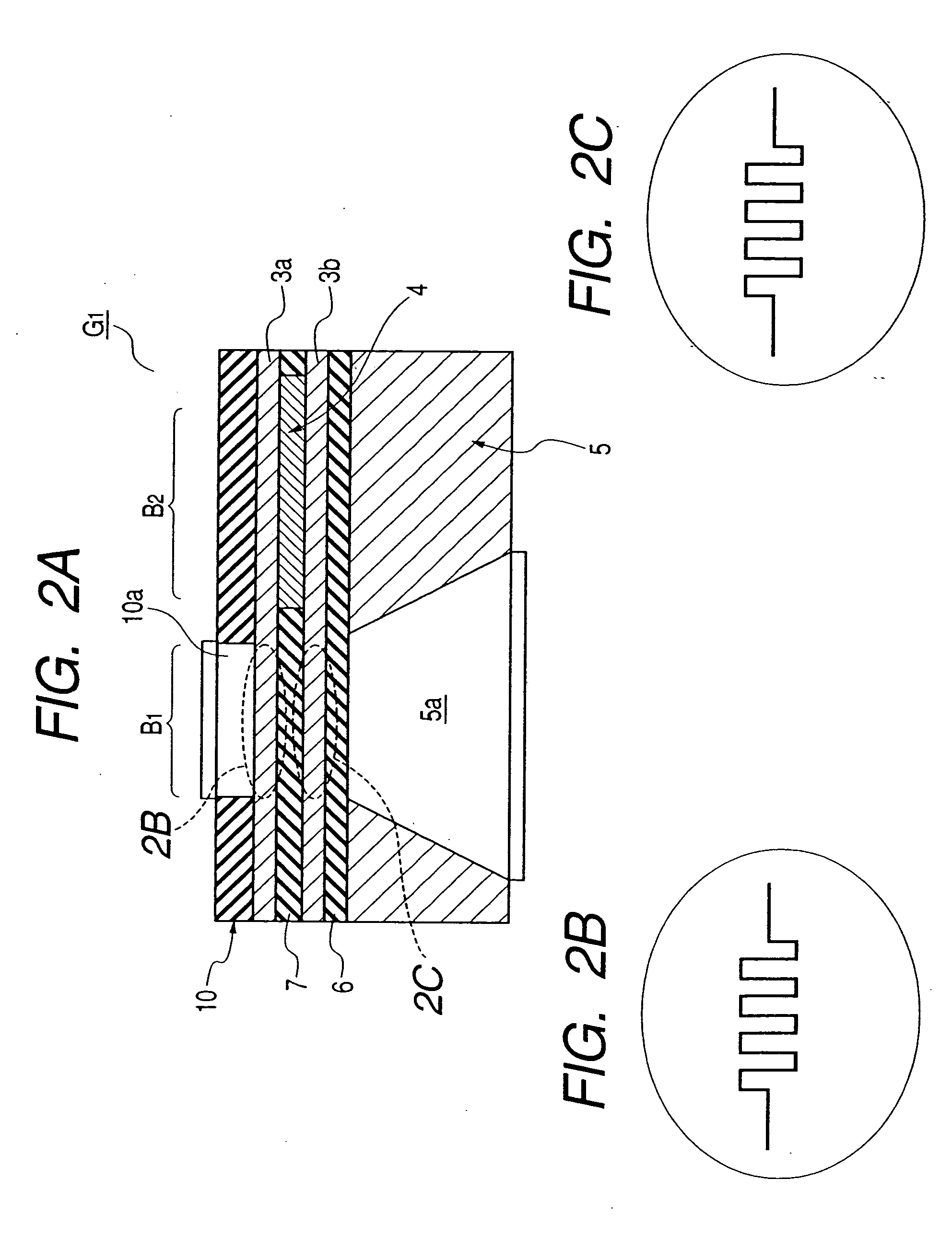
[0085] A media sensor G1 for detecting the humidity and mechanical properties of the sheet material P was structured as shown in FIG. 2A. In FIG. 2A, the insulating film 10 was formed on a surface of the upper electroconductive member 3a, and the hole portion 10a was formed in a portion of the insulating film 10 that corresponded to the detecting unit B1, thus avoiding a direct contact between the upper electroconductive member 3a and the sheet material P.
[0086] The insulating films 6 and 7 were each formed from silicon dioxide by RF sputtering to a thickness of 3 μm. The lower electroconductive member 3b was formed from Pt of 300 nm thicknesses by RF sputtering. A Ti film with a thickness of 50 nm was formed between the lower electroconductive member 3b and the insulating films 6 and 7. The metal oxide 4 was a PZT (Zr / Ti=36 / 65) film that was for...
example 3
[0098] In this example, a sheet identifying device (information detecting device) A3 shown in FIG. 10 was mounted to a copying machine (image forming apparatus).
[0099] The copying machine was equipped with: a sheet feeding cassette (first storage unit) for storing recording paper (a first sheet material); an image forming unit for forming an image on the recording paper; a paper transporting device (first sheet material transporting device) for transporting recording paper from the sheet feeding cassette to the image forming unit; an original table (second storage unit) on which an original (second sheet material) was placed; an image reading unit for reading an image of the original; an original transporting device (second sheet transporting device) for transporting the image to the image reading unit; an image control unit for controlling image formation conditions based on information from the sheet identifying device; and a sheet delivery tray (third storage unit) for storing r...
PUM
| Property | Measurement | Unit |
|---|---|---|
| weight | aaaaa | aaaaa |
| diameter | aaaaa | aaaaa |
| thickness | aaaaa | aaaaa |
Abstract
Description
Claims
Application Information


