[0016] It is therefore a primary object of the present invention to eliminate the aforementioned problems and to provide a semiconductor device having a ferroelectric capacitor having a small degradation in characteristics, and a method for manufacturing the same.
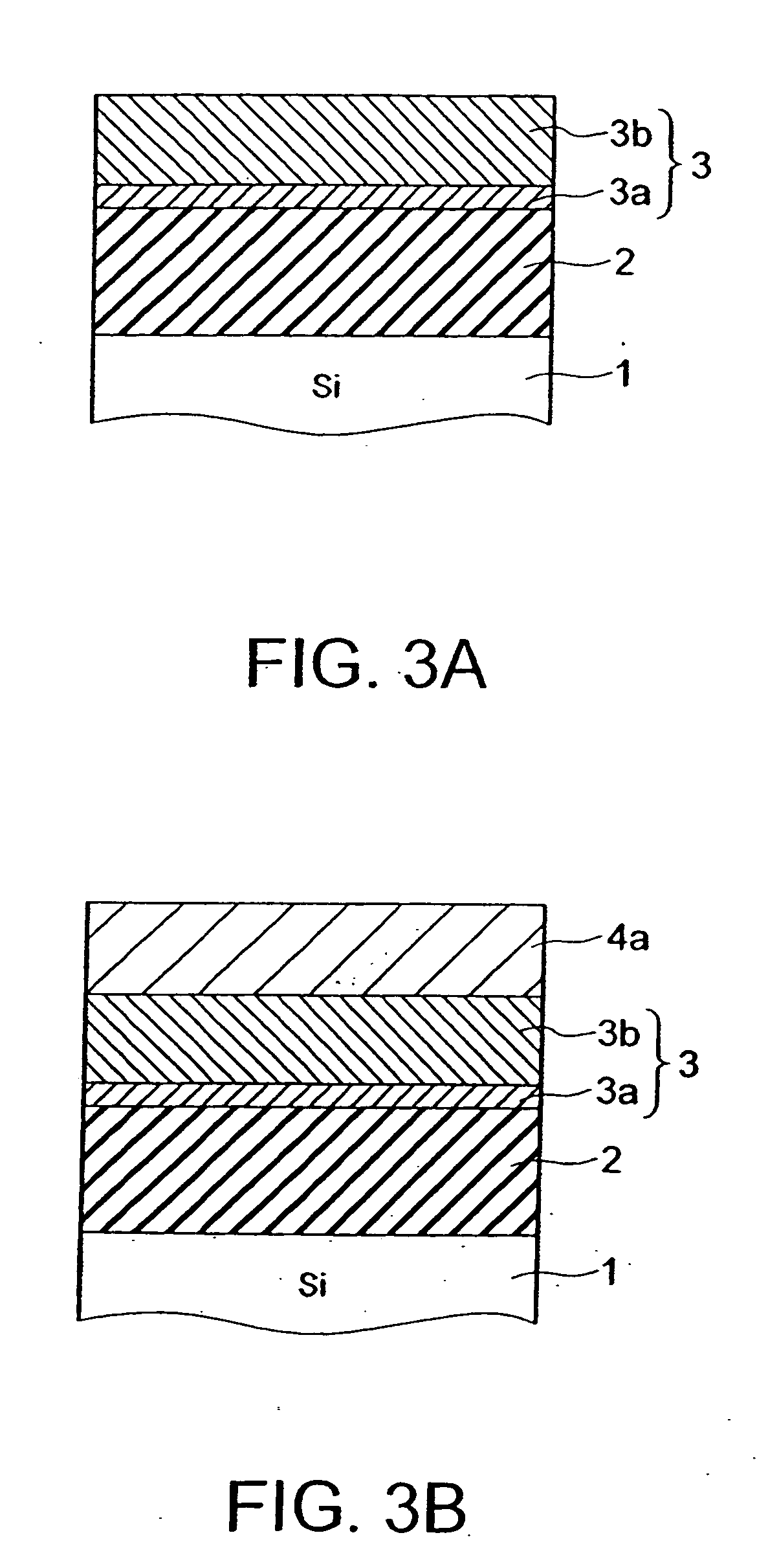
[0017] In a semiconductor integrated circuit according to one aspect of the present invention, the dielectric film of a capacitor has a two-layer structure, which comprises a first metal oxide, for example, BSTO(Ba1-xSrxTiO3), dielectric film on the side of a bottom electrode, and a second metal oxide dielectric film. The first metal oxide film is crystallized after it is deposited on the bottom electrode. If the dielectric film has such a stacked dielectric film structure, the constituent element of the bottom electrode is diffused in the first metal oxide film at the step of crystallizing the first metal oxide dielectric film, and the first metal oxide dielectric film is crystallized so as to contain the constituent element of the bottom electrode. Then, when the first metal oxide dielectric film is crystallized, the constituent element of the bottom electrode incorporated into the first metal oxide dielectric film can hardly move so that the constituent element of the bottom electrode is hardly diffused even at the step of crystallizing the second metal oxide dielectric film deposited on the first metal oxide dielectric film. In addition, if the second metal oxide dielectric film is crystallized before the top electrode is deposited, the constituent element of the top electrode is not diffused in the second metal oxide dielectric film. Therefore, in the case of a ferroelectric capacitor having first and second metal oxide films of ferroelectric films, the second metal oxide film has a good ferroelectric characteristic having no leak, so that it is possible to obtain a ferroelectric capacitor having a large spontaneous polarization. In addition, since the constituent element of the bottom electrode Is not diffused in the second metal oxide dielectric film, it is possible to easily decrease the thickness of the second metal oxide film.
[0018] Even in the case of a high-dielectric capacitor wherein each of the first and second metal oxide films is a high-dielectric film, it is possible to obtain an excellent capacitor characteristic having a small leak for the same reason, so that it is possible to decrease the thickness of the high-dielectric film.
[0020] In a semiconductor integrated circuit according to another aspect of the present invention, in addition to the first and second metal oxide dielectric films described above, a third metal oxide dielectric film is provided between the above described second metal oxide dielectric film and the top electrode. In this case, if the third metal oxide dielectric film is crystallized after the top electrode is deposited thereon, the third metal oxide dielectric film is crystallized so as to contain the constituent element of the top electrode similar to the first metal oxide dielectric film. Therefore, the third metal oxide dielectric film serves as a metallic layer against the reducing power due to hydrogen or the like from the top of the second metal oxide dielectric film. Thus, it is possible to more effectively inhibit the characteristics of the ferroelectric capacitor from being degraded by the reducing gas.
[0021] It is a further object of the present invention to provide a semiconductor device having a ferroelectric capacitor which can effectively inhibit the damage to the layer between a ferroelectric film and a bottom electrode, and the peeling of films and which can reduce the degradation in remnant polarization, and a method for manufacturing the same.
[0022] In the ferroelectric capacitor according to the present invention, although the bottom electrode is patterned so as to extend to the outside of the ferroelectric film, a part of the surface portion of the bottom electrode is removed by over etching when the ferroelectric film is patterned, so that the level of the surface of the extending portion of the bottom electrode is lower than that of the layer between the ferroelectric film and the bottom electrode. Moreover, the protective film against hydrogen gas and a halogen gas is formed so as to cover a region extending from the surface of the bottom electrode to the sides of the ferroelectric film and top electrode. Thus, it is possible to effectively inhibit the reducing element from penetrating into the layer between the ferroelectric film and the bottom electrode, so that it is possible to obtain a reliable ferroelectric capacitor, the remnant polarization of which does not decrease, which will result in improvement of electrical property for FRAMS, and decrease of leak of charges and improvement in adaptability for scaling for DRAM

