Ferroelectric memory device having a hydrogen barrier film

a technology of ferroelectric capacitors and memory devices, which is applied in the direction of capacitors, solid-state devices, transistors, etc., can solve the problems of reducing the reliability and yield of the whole memory, the failure of the memory, and the inability to achieve real-time techniques, so as to reduce the degradation of remnant polarization, effectively inhibit the characteristics of the ferroelectric capacitor, and reduce the effect of degradation

Inactive Publication Date: 2006-01-03
KK TOSHIBA
View PDF22 Cites 28 Cited by
  • Summary
  • Abstract
  • Description
  • Claims
  • Application Information

AI Technical Summary

Benefits of technology

[0016]It is therefore a primary object of the present invention to eliminate the aforementioned problems and to provide a semiconductor device having a ferroelectric capacitor having a small degradation in characteristics, and a method for manufacturing the same.
[0017]In a semiconductor integrated circuit according to one aspect of the present invention, the dielectric film of a capacitor has a two-layer structure, which comprises a first metal oxide, for example, BSTO(Ba1−xSrxTiO3), dielectric film on the side of a bottom electrode, and a second metal oxide dielectric film. The first metal oxide film is crystallized after it is deposited on the bottom electrode. If the dielectric film has such a stacked dielectric film structure, the constituent element of the bottom electrode is diffused in the first metal oxide film at the step of crystallizing the first metal oxide dielectric film, and the first metal oxide dielectric film is crystallized so as to contain the constituent element of the bottom electrode. Then, when the first metal oxide dielectric film is crystallized, the constituent element of the bottom electrode incorporated into the first metal oxide dielectric film can hardly move so that the constituent element of the bottom electrode is hardly diffused even at the step of crystallizing the second metal oxide dielectric film deposited on the first metal oxide dielectric film. In addition, if the second metal oxide dielectric film is crystallized before the top electrode is deposited, the constituent element of the top electrode is not diffused in the second metal oxide dielectric film. Therefore, in the case of a ferroelectric capacitor having first and second metal oxide films of ferroelectric films, the second metal oxide film has a good ferroelectric characteristic having no leak, so that it is possible to obtain a ferroelectric capacitor having a large spontaneous polarization. In addition, since the constituent element of the bottom electrode Is not diffused in the second metal oxide dielectric film, it is possible to easily decrease the thickness of the second metal oxide film.
[0018]Even in the case of a high-dielectric capacitor wherein each of the first and second metal oxide films is a high-dielectric film, it is possible to obtain an excellent capacitor characteristic having a small leak for the same reason, so that it is possible to decrease the thickness of the high-dielectric film.
[0020]In a semiconductor integrated circuit according to another aspect of the present invention, in addition to the first and second metal oxide dielectric films described above, a third metal oxide dielectric film is provided between the above described second metal oxide dielectric film and the top electrode. In this case, if the third metal oxide dielectric film is crystallized after the top electrode is deposited thereon, the third metal oxide dielectric film is crystallized so as to contain the constituent element of the top electrode similar to the first metal oxide dielectric film. Therefore, the third metal oxide dielectric film serves as a metallic layer against the reducing power due to hydrogen or the like from the top of the second metal oxide dielectric film. Thus, it is possible to more effectively inhibit the characteristics of the ferroelectric capacitor from being degraded by the reducing gas.
[0021]It is a further object of the present invention to provide a semiconductor device having a ferroelectric capacitor which can effectively inhibit the damage to the layer between a ferroelectric film and a bottom electrode, and the peeling of films and which can reduce the degradation in remnant polarization, and a method for manufacturing the same.
[0022]In the ferroelectric capacitor according to the present invention, although the bottom electrode is patterned so as to extend to the outside of the ferroelectric film, a part of the surface portion of the bottom electrode is removed by over etching when the ferroelectric film is patterned, so that the level of the surface of the extending portion of the bottom electrode is lower than that of the layer between the ferroelectric film and the bottom electrode. Moreover, the protective film against hydrogen gas and a halogen gas is formed so as to cover a region extending from the surface of the bottom electrode to the sides of the ferroelectric film and top electrode. Thus, it is possible to effectively inhibit the reducing element from penetrating into the layer between the ferroelectric film and the bottom electrode, so that it is possible to obtain a reliable ferroelectric capacitor, the remnant polarization of which does not decrease, which will result in improvement of electrical property for FRAMS, and decrease of leak of charges and improvement in adaptability for scaling for DRAM

Problems solved by technology

However, in the conventional ferroelectric capacitor using PZT, hydrogen causes the decreases of the amount of spontaneous polarization, so that the signal margin in FRAM is decreased resulting in the bit failure of the memory, and the decrease of reliability and yield of the whole memory.
On the other hand, although a technique for improving the characteristics of a ferroelectric capacitor by decreasing the concentration of hydrogen in the ferroelectric capacitor is disclosed in, e.g., Japanese Patent Laid-Open No. 8-8404(1996), this technique is not realistic since there is a strict limit to a process.
Therefore, it is difficult to carry out the scaling of the thickness of the ferroelectric film.
However, if it is intended to obtain such a shape of capacitor, there is a problem in that Pt splashed by etching the bottom Pt electrode 72 is adhered to the side wall of the PZT film 73 again to form a Pt fence to establish a short-circuit between the top and bottom electrodes.
However, in the shape that the layer between the PZT film 73 and the bottom Pt electrode 72 is continued from the surface of the bottom Pt electrode 72 extending to the outside of the PZT film 73 as shown in FIG. 2, even if the hydrogen protecting film is provided, it is difficult to interrupt the reducing element, such as hydrogen, which penetrates into the layer between the PZT film 73 and the bottom Pt electrode 72 along the surface of the bottom Pt electrode 72, so that it is not possible to surely prevent the degradation in characteristics.

Method used


Image

  • Ferroelectric memory device having a hydrogen barrier film
  • Ferroelectric memory device having a hydrogen barrier film
  • Ferroelectric memory device having a hydrogen barrier film

Examples


Embodiment Construction

[0082]Referring now to the accompanying drawings, the preferred embodiments of the present invention will be described below.

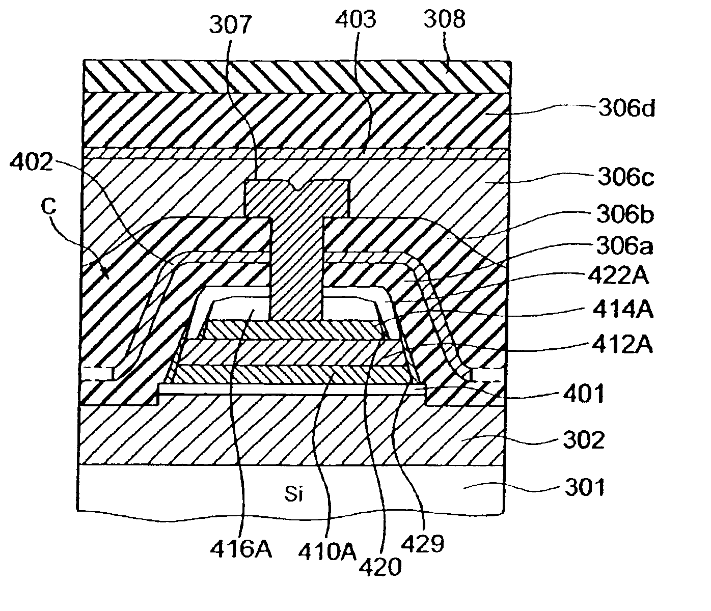
[0083]In the following description, most of the embodiments show only the capacitor part. It is to be noted that contact plugs, interconnections, MOS transistors, etc. are generally provided as shown in FIG. 15 which will be described later, but in other Figures, they are omitted.

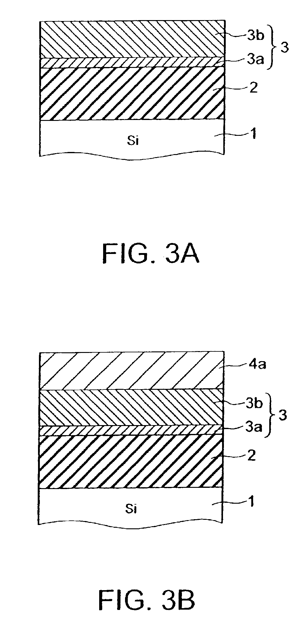
[0084]FIGS. 3A through 3E show a process for manufacturing a first preferred embodiment of a ferroelectric capacitor on a silicon substrate. In FIG. 3A, elements, such as MOS transistors, are formed on a silicon substrate 1, and a silicon oxide (SiO2) film 2 for covering the MOS transistor is formed thereon. On the silicon oxide film 2, an adhesion film 3a having a thickness of 20 nm is deposited by a sputtering method, and subsequently, a Pt film 3b having a thickness of 20 nm is deposited by a sputtering method to form a bottom electrode 3 of a Pt / adhesion stacked film.

[0085]Subsequ...


PUM


Abstract

There is provided a semiconductor device having a ferroelectric capacitor formed on a semiconductor substrate covered with an insulator film, wherein the ferroelectric capacitor comprises: a bottom electrode formed on the insulator film; a ferroelectric film formed on the bottom electrode; and a top electrode formed on the ferroelectric film. The ferroelectric film has a stacked structure of either of two-layer-ferroelectric film or three-layer-ferroelectric film. The upper ferroelectric film is metallized and prevents hydrogen from diffusing in lower ferroelectric layer. Crystal grains of the stacked ferroelectric films are preferably different.

Description

CROSS-REFERENCE TO RELATED APPLICATION[0001]This application is a divsional of U.S. patent application Ser. No. 09 / 359,324 filed Jul. 23, 1999, now U.S. Pat. No. 6,586,790, which is based upon and claims the benefit of priority from the prior Japanese Patent Application Nos. 208999 / 1998, filed Jul. 24, 1998; 324254 / 1998, filed Nov. 13, 1998; and 345368 / 1998, filed Dec. 4, 1998, the entire contents of which are incorporated herein by reference.BACKGROUND OF THE INVENTION[0002]1. Field of the Invention[0003]The present invention relates generally to a semiconductor device including a ferroelectric capacitor having a thin-film structure and a method of manufacturing the same.[0004]2. Related Background Art[0005]There is known a non-volatile semiconductor memory device using a ferroelectric capacitor (which will be hereinafter referred to as a “ferroelectric memory”). The ferroelectric capacitor is formed by stacking a bottom electrode, a ferroelectric film and a top electrode on a subs...

Claims


Application Information

Patent Timeline
Patent Type & Authority Patents(United States)
IPC IPC(8): H01L29/76H01L31/113H01L31/119H01L29/94H01L31/062H01L21/02H01L21/8246H01L27/115
CPCH01L27/11502H01L27/11507H01L28/65H01L28/57H01L28/56H10B53/30H10B53/00
Inventor KANAYA, HIROYUKIKUNISHIMA, IWAOYAMAKAWA, KOJIIWAMOTO, TSUYOSHIMOCHIZUKI, HIROSHIKUMURA, YOSHINORI
Owner KK TOSHIBA
Why Eureka
Try Eureka