Semiconductor device and manufacturing method of the same

a semiconductor and manufacturing method technology, applied in semiconductor devices, semiconductor/solid-state device details, electrical devices, etc., can solve the problems of uneven deformation of the opening portion of the resist, the inability to easily perform selective etching of the silicon nitride film using the resist as a mask, and the inability to raise the selective ratio between the resist and the silicon nitride film

Inactive Publication Date: 2006-01-26
KK TOSHIBA
View PDF16 Cites 18 Cited by
  • Summary
  • Abstract
  • Description
  • Claims
  • Application Information

AI Technical Summary

Problems solved by technology

Since the etching selective ratio between the resist and the silicon nitride film cannot be raised, selective etching of the silicon nitride film using the resist as a mask cannot easily be performed.
This leads to a fact that the opening portions in the resist are unevenly deformed.
Therefore, a plurality of trenches each having a smooth inner surface and exhibiting satisfactory accuracy cannot easily be formed with a high yield in the semiconductor substrate.
Since so-called film thinning occurs when the dry etching is performed, the trenches cannot easily be formed.
In the portions of low density device regions, the number of silicon nitride film stoppers is insufficiently small.
Thus, the silicon oxide film is excessively polished in the smoothing process.
As a result, there arises a problem in that smoothing and formation of the device regions cannot be performed uniformly over the overall surface of the wafer.
The smoothing step, however, sometimes encounters a crack in the silicon oxide film in the low density portion.
When the silicon nitride film stoppers on the device region and the polysilicon mask are removed, there arises a problem in that the silicon substrate is scooped out excessively.
If the surface of the wafer has an uneven portion, the projecting portions of the surface of the wafer are excessively etched when the pattern of the silicon nitride film is formed.
As a result, the metallic film formed below the pattern is undesirably etched, causing a problem to arise in that a gate electrode formation cannot be satisfactorily performed.
Therefore, the edge line portion of the gate electrode is undesirably etched when the contact hole is opened in the SAC formation step.
Thus, the gate metal is exposed to the outside, causing a short-circuit fault to occur when the metal for the metallization is buried in the contact hole.
As a result, it is known that the SAC cannot easily be formed in the process for manufacturing E2 PROM in which the gate electrode has a high aspect ratio (the ratio of the length of the gate and the height of the gate).
Hitherto, it is very difficult to control the depth of the trenches in the surface of the wafer when the trenches are formed in the interlayer insulating film.
Therefore, the wiring capacitance is enlarged excessively, causing the operation speed of the semiconductor device to be reduced.
Therefore, the wiring metal cannot be easily buried in the trench.
Therefore, there arises a problem in that a fault in burying and a short-circuit fault of the wiring metal occur.
When the resist is removed by performing O2 ashing after the pattern has been formed, a phenomenon undesirably occurs in that polysilane is oxidized.
Thus, oxidized polysilane cannot easily be removed.
However, with progress in the degree of miniaturization, the operating speed and the multi-layered structure, the signal transmission delay caused by the so-called “inter-wiring parasitic capacitance” and the wiring resistance is brought about as a serious problem.
However, with further progress in the degree of miniaturization of the semiconductor device in the future, it is expected that it will be difficult to cope with the signal transmission delay caused by the inter-wiring parasitic capacitance and the wiring resistance by simply employing the wiring structure using the low-k material and Cu in combination.
Also, an additional problem is generated that the processing of the insulating film and the burying of the wiring material will be rendered difficult.

Method used


Image

  • Semiconductor device and manufacturing method of the same
  • Semiconductor device and manufacturing method of the same
  • Semiconductor device and manufacturing method of the same

Examples


tenth embodiment

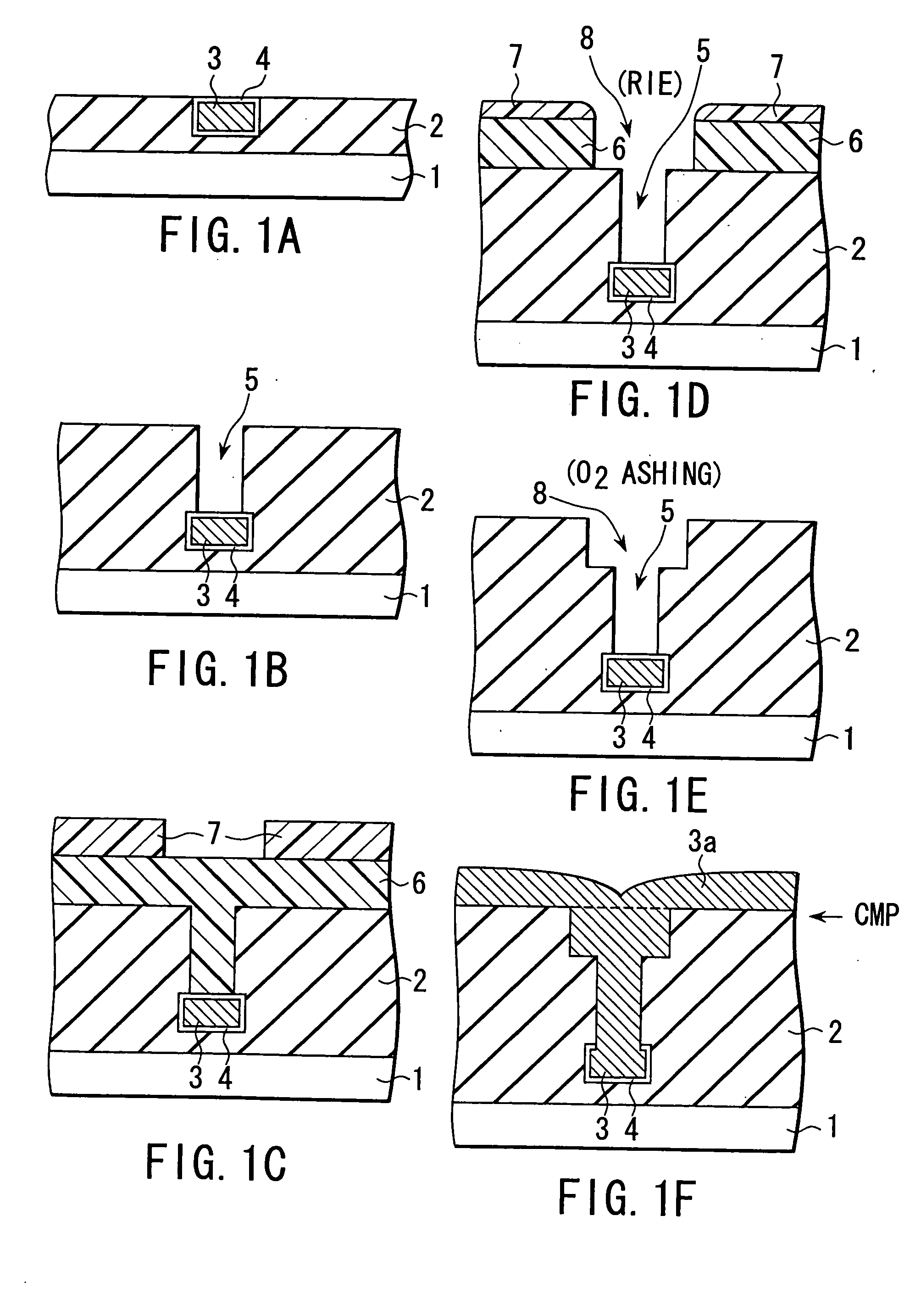
[0223] Referring to FIGS. 12A and 12B, a tenth embodiment of the present invention will now be described. The tenth embodiment is different from the eighth embodiment in that the anti-reflective film constituted by the polysilane 6 is made to be a portion of the insulating film 2 after the contact hole 5 has been formed.

[0224] As shown in FIG. 12A, a thick insulating film 2 is directly formed on the silicon substrate 1. Then, the anti-reflective film constituted by the polysilane 6 is applied. Then, the pattern of the resist 7 having an opening portion of the contact hole is formed on the anti-reflective film.

[0225] The resist 7 is used as the etching mask to perform anisotropic RIE to open the contact hole 5 that reaches the surface of the silicon substrate 1. Then, as shown in FIG. 12B, O2 ashing is performed to remove the resist 7. Simultaneously, the polysilane 6 is changed to the silicon oxide film. Thus, the anti-reflective film can be formed to be a portion of the insulatin...

eleventh embodiment

[0229] Referring to FIGS. 13A to 13C, an eleventh embodiment of the present invention will now be described. As shown in FIG. 13A, the thick insulating film 2 is formed on the silicon substrate 1. Then, an anti-reflective film constituted by the polysilane 6 is applied. Then, the pattern of the resist 7 having the opening portion of the contact hole is formed. Then, the resist 7 is used as a mask when the anisotropic RIE is performed to open the polysilane 6. Then, as shown in FIG. 13B, N2 ashing is performed to remove the resist 7. Simultaneously, the polysilane 6 is changed to the silicon nitride film.

[0230] Then, as shown in FIG. 13C, the silicon nitride film 4 is used as the mask when the anisotropic RIE is performed to form the contact hole having a high aspect ratio which reaches the silicon substrate 1.

[0231] When a resist mask is directly used to form the contact hole having the high aspect ratio by the anisotropic RIE, the film thinning of the resist mask occurs. On the o...

twelfth embodiment

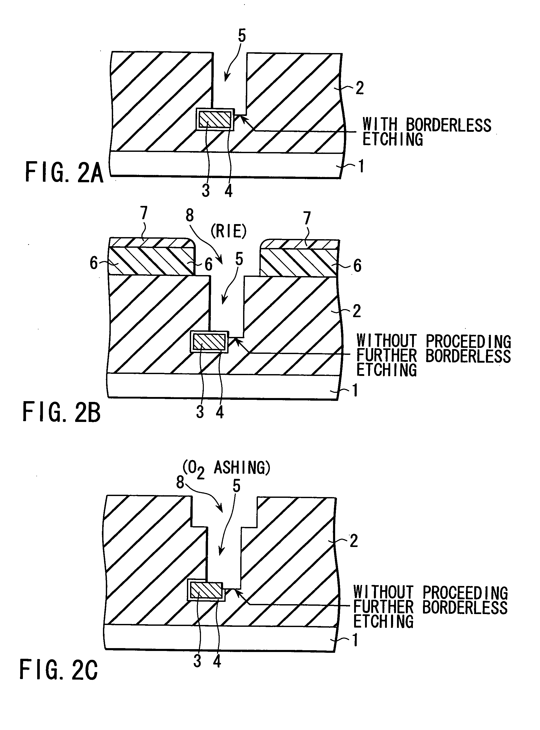
[0233] Referring to FIGS. 14A to 14C, a twelfth embodiment of the present invention will now be described. As shown in FIG. 14A, the insulating film 2 constituted by the thick silicon oxide film is formed on the silicon substrate 1. Then, the anti-reflective film constituted by the polysilane 6 is applied to the surface of the insulating film 2. The resist 7 is used to form a reversed pattern of the resist 7 such that the opening portion of the contact hole is covered. Then, RIE using N2 is performed to change the exposed surface of the silicon nitride film 4, and then the resist 7 is removed.

[0234] Then, as shown in FIG. 14B, the silicon nitride film 4 is used as a mask to perform the anisotropic RIE to open the contact hole, which reaches the silicon substrate 1, in the insulating film 2 constituted by the polysilane 6 and the silicon oxide film.

[0235] Then, a treatment similar to the O2 ashing step is performed to change the polysilane 6 to the silicon oxide film. Thus, the pol...


PUM


Abstract

A semiconductor device is disclosed, which comprises a semiconductor substrate, a semiconductor element formed on the semiconductor substrate, and multi-level wiring structure including first wirings at a plurality of levels, in which the first wirings at at least one of the levels are provided at different heights in a cross-sectional view of the multi-level wiring structure, and extend to cross at an oblique angle with the first wirings at an adjacent level in a plan view.

Description

CROSS-REFERENCE TO RELATED APPLICATIONS [0001] This application is a Continuation-in-Part of U.S. patent application Ser. No. 10 / 983,746, filed Nov. 9, 2004, which is a divisional of U.S. patent application Ser. No. 10 / 086,556, filed Mar. 4, 2004 (now U.S. Pat. No. 6,849,923), which is a Continuation-in-Part of U.S. patent application Ser. No. 09 / 995,839, filed Nov. 29, 2001 (now U.S. Pat. No. 6,605,542), which is a continuation of U.S. patent application Ser. No. 09 / 522,175, filed Mar. 9, 2000 (now U.S. Pat. No. 6,352,931), which is based upon and claims the benefit of priority from prior Japanese Patent Application No. 11-066293, filed Mar. 12, 1999, the entire contents of which are incorporated herein by reference.BACKGROUND OF THE INVENTION [0002] 1. Field of the Invention [0003] The present invention relates to a manufacturing method of semiconductor devices by using a dry etching technology. More particularly, the present invention relates to a method of forming an interlayer ...

Claims


Application Information

Patent Timeline
Patent Type & Authority Applications(United States)
IPC IPC(8): H01L23/48
CPCH01L21/0276H01L2924/30107H01L21/31058H01L21/31111H01L21/31116H01L21/31138H01L21/31144H01L21/3121H01L21/32139H01L21/76801H01L21/76802H01L21/76808H01L21/7681H01L21/76811H01L21/76819H01L21/76825H01L21/76826H01L21/76831H01L21/76834H01L21/76843H01L21/76847H01L21/76897H01L21/823425H01L21/823475H01L23/522H01L23/5329H01L21/3081H01L2924/0002H01L21/02211H01L21/02164H01L2924/00
Inventor SETA, SHOJISEKINE, MAKOTONAKAMURA, NAOFUMI
Owner KK TOSHIBA
Why Eureka
Try Eureka