Bonding configuration structure for facilitating electrical testing in a bonding process and a testing method using the same

Active Publication Date: 2006-01-26
AU OPTRONICS CORP
View PDF3 Cites 16 Cited by
  • Summary
  • Abstract
  • Description
  • Claims
  • Application Information

AI Technical Summary

Benefits of technology

[0006] It is therefore an object of the invention to provide a bonding configuration structure for facilitating electrical testing and a method thereof in the bonding process. By means of quantifying t

Problems solved by technology

However, the process of manufacturing the liquid crystal display is more complicated than that of manufacturing the CRT display.
However, qualitative determination by manual inspection without quantitative analysis is subjective.
Therefore, the defects

Method used


Image

  • Bonding configuration structure for facilitating electrical testing in a bonding process and a testing method using the same
  • Bonding configuration structure for facilitating electrical testing in a bonding process and a testing method using the same
  • Bonding configuration structure for facilitating electrical testing in a bonding process and a testing method using the same

Examples


Example

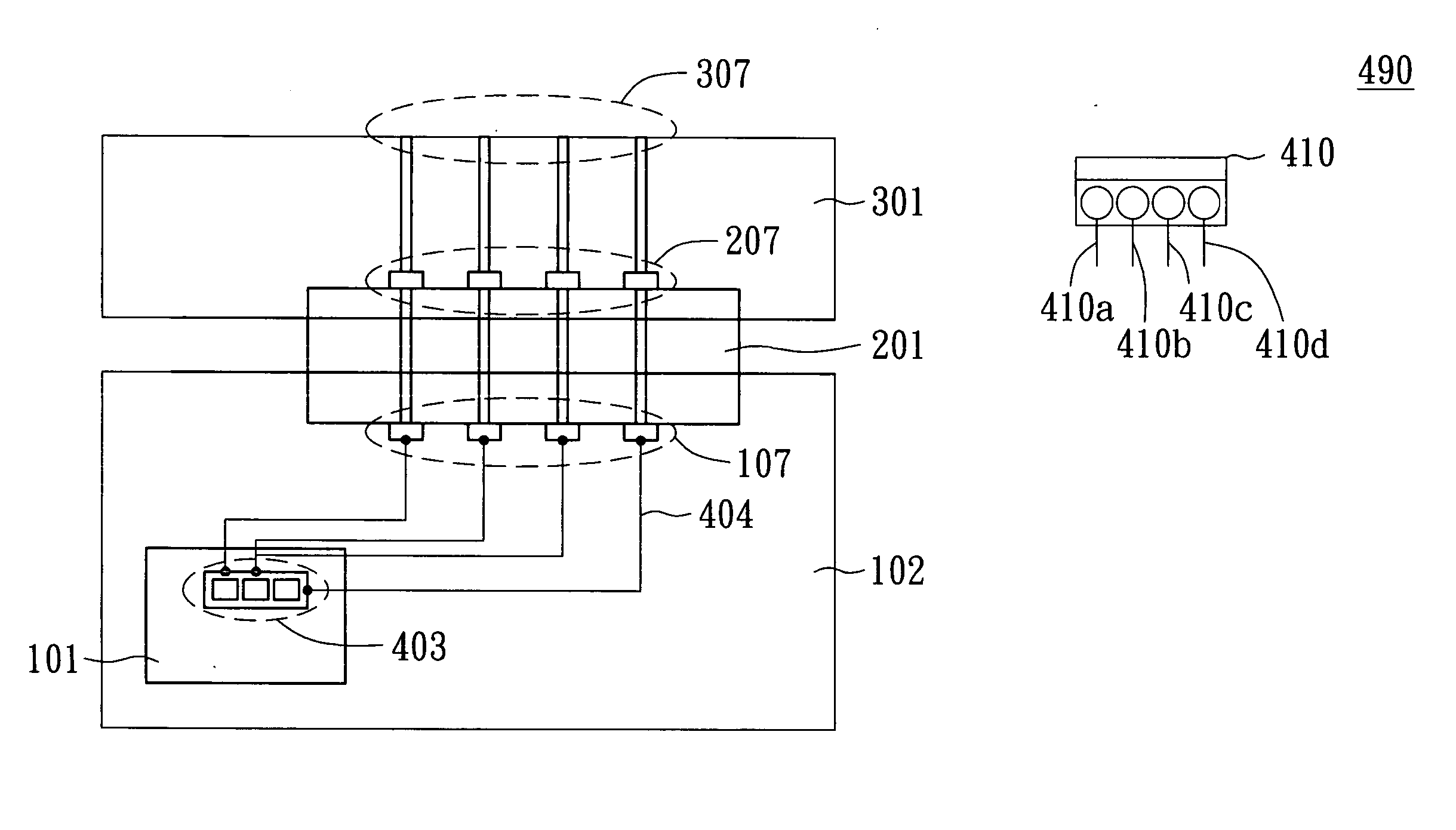
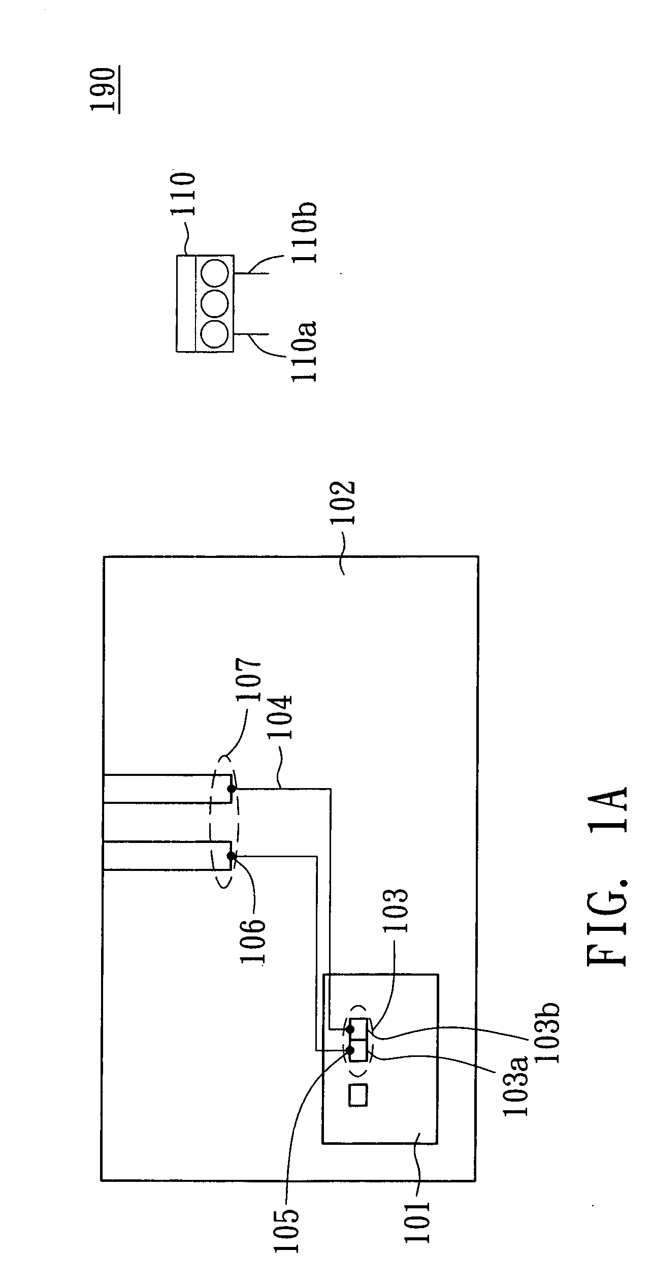
[0019] Referring to FIG. 1A, a top view of a bonding configuration structure in the bonding process according to a first embodiment is shown. The bonding configuration structure 190 includes a bonded component, a bonding component, a bond portion 103, and a leading component 104. An electrical testing device 110 is also provided for testing the electrical characteristic of the bonding configuration structure 190. In the first embodiment, the bonded component is a glass substrate 102, and the bonding component is a driver integrated circuit 101. The leading component 104 has a first end 105 and a second end 106. The first end 105 is coupled to the bond portion 103, and the second end 106 is disposed on the glass substrate 102 to form a first testing portion 107. The first testing portion 107 can be a lead or a pin. The bond portion 107 connects the leading component 104 and the driver integrated circuit 101.

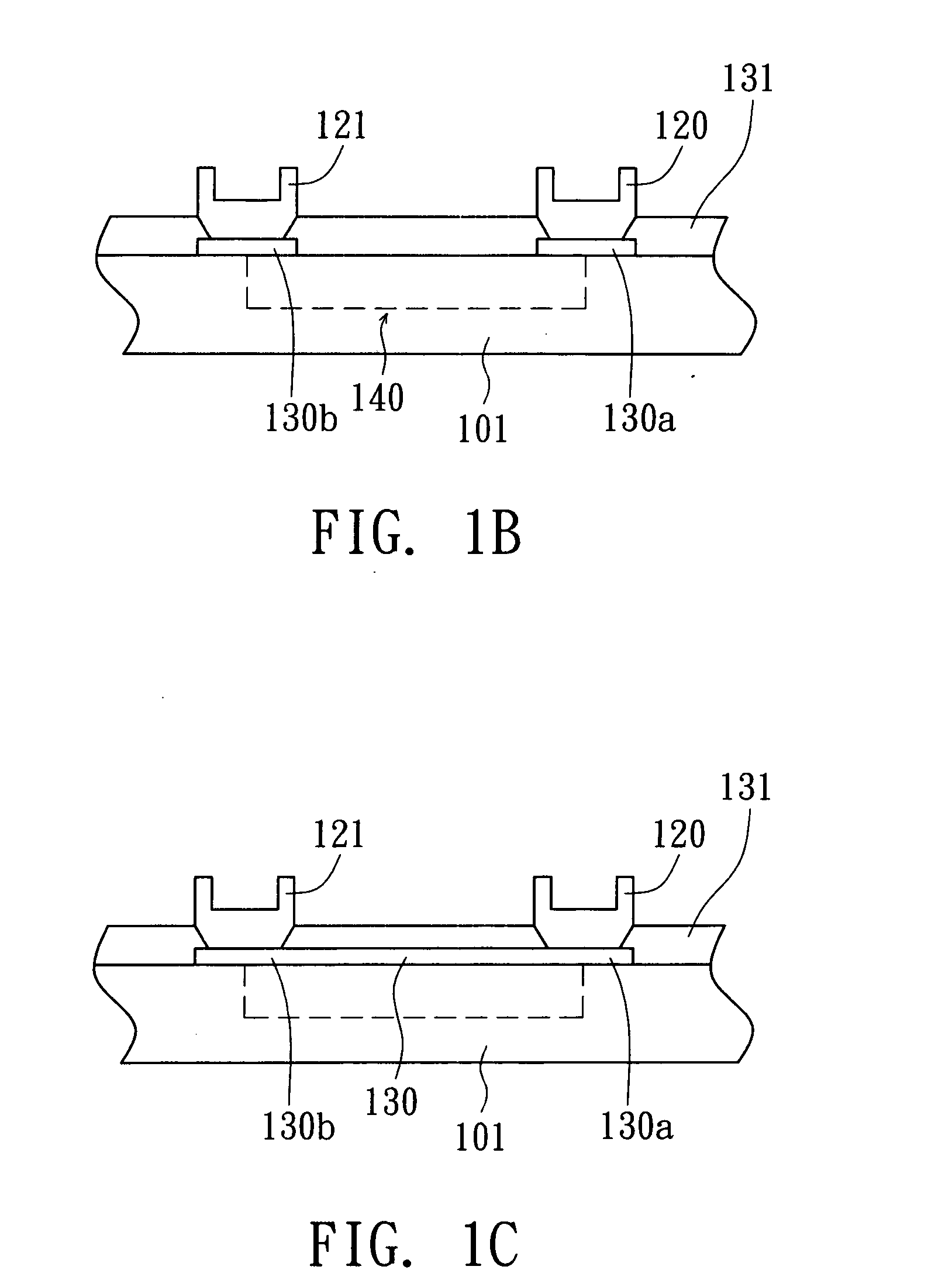
[0020] Referring to FIG. 1B, a cross-sectional view of a bond portion in FIG...


PUM

PropertyMeasurementUnit
Structureaaaaaaaaaa
Electrical resistanceaaaaaaaaaa
Flexibilityaaaaaaaaaa

Abstract

A bonding configuration structure for facilitating electrical testing in a bonding process and a testing method are provided. The bonding configuration includes a bonded component, a bonding component, a bond portion and a leading component. The bonding component is disposed on the bonded component. The bonding component has a first end and a second end. The first end is coupled to the bond portion. The second end is disposed on the bonded component to form the first testing portion.

Description

[0001] This application claims the benefit of Taiwan application Ser. No. 93122335, filed Jul. 26, 2004, the subject matter of which is incorporated herein by reference. BACKGROUND OF THE INVENTION [0002] 2. Field of the Invention [0003] The invention relates in general to a bonding configuration structure and a testing method thereof, and more particularly to a bonding configuration structure and a testing method for facilitating electrical testing in a bonding process. [0004] 2. Description of the Related Art [0005] Currently, the liquid crystal display is gradually becoming the mainstream of all the displays, mainly because that the liquid crystal display occupied the smaller space than the conventional CRT display. However, the process of manufacturing the liquid crystal display is more complicated than that of manufacturing the CRT display. The reason for the above situation is that every steps of the procedure takes high skill and concern while producing the electrical product...

Claims


Application Information

Patent Timeline
IPC IPC(8): B23K31/12G01R31/04G01R1/073G01R27/02G01R31/01
CPCG01R1/07378
Inventor CHEN, HUI-CHANGLEE, CHUN-YU
Owner AU OPTRONICS CORP
Why Eureka
Try Eureka