Solid-state imaging device, production method and drive method thereof, and camera

a solid-state imaging and drive method technology, applied in the field of cameras, can solve the problems of delay of a transfer pulse applied, inability to detect the incident light, so as to reduce the blocking of an incident light, reduce the blocking of the incident light, and increase the angle of view

Active Publication Date: 2006-02-02
SONY CORP
View PDF8 Cites 13 Cited by
  • Summary
  • Abstract
  • Description
  • Claims
  • Application Information

AI Technical Summary

Benefits of technology

[0015] It is desired to provide a solid-state imaging device for reducing blocking of an incident light at a circumferential portion of a light receiving portion and attaining a larger angle of view and high-speed driving.

Problems solved by technology

It is because such the transfer electrode is generally composed as a distributed constant circuit of an RC, and a high resistance of the transfer electrode will result in non-sharpness (dulling) and delay of a transfer pulse applied by the transfer electrode to disturb a transfer of CCD charges.
Such the shunt wiring in the vertical direction suffers from the disadvantages that the transfer mode is limited and multi-phase driving used for interleaving transfer of pixels is hard to be realized.
However, an incident light to the light receiving portion is blocked by the transfer electrode itself, so that there has been a proposal of reducing a thickness and projections of the transfer electrode.
However, the circumstances are that a CCD with a larger angle of view and a CCD with high-speed transfer, etc. are actually hard to be realized only by the well-known single-layer transfer electrode configuration, and an eclipse of an incident light cannot be sufficiently reduced.

Method used


Image

  • Solid-state imaging device, production method and drive method thereof, and camera
  • Solid-state imaging device, production method and drive method thereof, and camera
  • Solid-state imaging device, production method and drive method thereof, and camera

Examples


first embodiment

[0037] First Embodiment

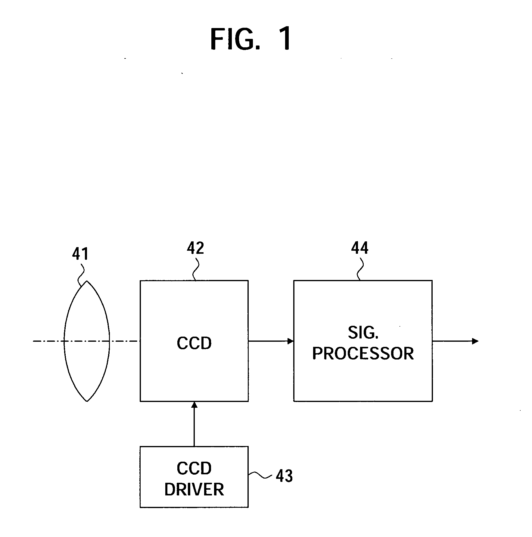
[0038]FIG. 1 is a schematic view of a camera of an embodiment of the present invention.

[0039] The camera shown in FIG. 1 includes an optical lens system 41, a charge-coupled device (CCD) 42, a CCD driver 43 and a signal processor 44.

[0040] The optical lens system 41 may include an objective lens, and an automatic-focusing and / or automatic exposure adjusting lens and mechanism. In the embodiment, the optical lens system 41 may include a shutter and a stop. The optical lens system 41 receives a light of an image and outputs the same to the CCD 42 to be focused thereat.

[0041] The CCD 42 and the CCD driver 43 cooperate to convert the incident light to the CCD 42 to an electric signal.

[0042] The signal processor 44 receives the converted electric signal indicating the image and carries out the image processing to recover the image, for example. Details of the CCD 42 and CCD driver 43 will be described.

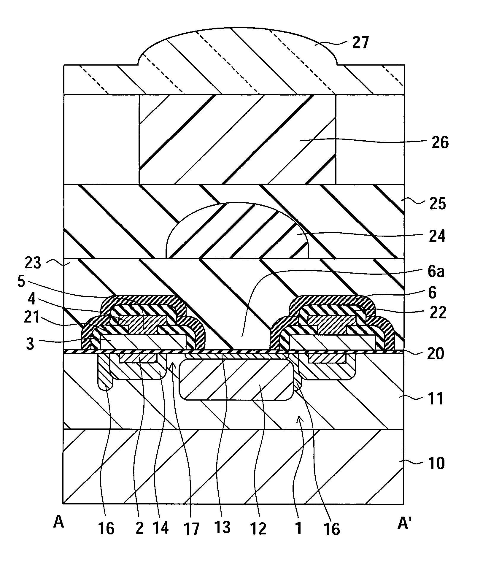
[0043] As an example of the CCD 42 shown in FIG. 1, a four-...

second embodiment

[0086] [Second Embodiment]

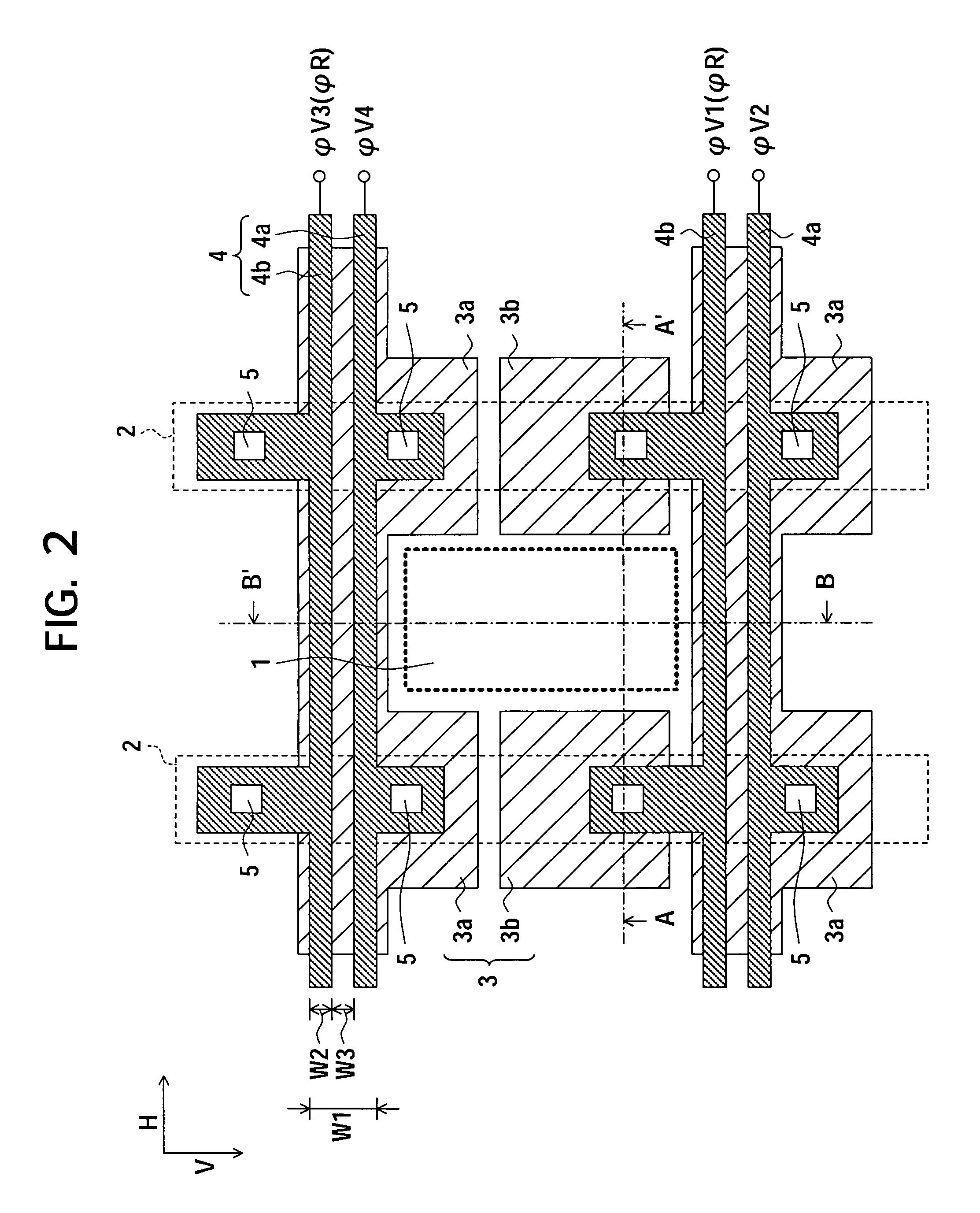
[0087] An example of the four-phase driving CCD was explained in the first embodiment, while in the present embodiment, an example of a six-phase driving or three-phase driving CCD, wherein the CCD 42 and the CCD driver 43 cooperate for performing three-phase driving, will be explained. FIG. 8 is a plan view of a main part of a pixel portion in a solid-state imaging device according to the second embodiment. Note that the same reference numbers are given to the same components as those in FIG. 2 and explanations thereof will be omitted.

[0088] In the transfer channel 2 extending in the vertical direction V, the transfer electrodes 3 made by single-layer polysilicon are arranged. In the present embodiment, the transfer electrodes 3 includes third transfer electrodes 3c in addition to the first transfer electrodes 3a and the second transfer electrodes 3b. A film thickness of the transfer electrodes 3 is preferably thin as, for example, 200 nm or thinner to pr...


PUM


Abstract

A solid-state imaging device capable of reducing an eclipse (blocking) of an incident light at a circumferential portion of a light receiving portion and realizing a larger angle of view and high-speed driving. A single-layer transfer electrode configuration of forming first transfer electrodes and second transfer electrodes by one polysilicon layer is adopted. Two shunt wirings extending in a horizontal direction are formed on the first transfer electrodes connected in a horizontal direction and, for example, four-phase transfer pulses are supplied to first transfer electrodes and second transfer electrodes on transfer channels through low-resistance shunt wirings extending in the horizontal direction.

Description

CROSS REFERENCES TO RELATED APPLICATIONS [0001] The present invention contains subject matter related to Japanese Patent Application JP 2004-221981 filed in the Japanese Patent Office on Jul. 29, 2004, the entire contents of which being incorporated herein by reference. BACKGROUND OF THE INVENTION [0002] 1. Field of the Invention [0003] The present invention relates to a camera, a solid-state imaging device used therefor such as a charge coupled device (CCD) type solid-state imaging device, and a method thereof. [0004] 2. Description of the Related Art [0005] To achieve a larger angle of view and transfer at a high-speed rate of a CCD solid-state imaging device, there are demanded a lowering a resistance of transfer electrode. It is because such the transfer electrode is generally composed as a distributed constant circuit of an RC, and a high resistance of the transfer electrode will result in non-sharpness (dulling) and delay of a transfer pulse applied by the transfer electrode t...

Claims


Application Information

Patent Timeline
Patent Type & Authority Applications(United States)
IPC IPC(8): H01L31/062H01L21/00H01L27/148H04N5/372
CPCH01L27/14843H01L27/14812H01L27/148
Inventor KANBE, HIDEO
Owner SONY CORP
Why Eureka
Try Eureka