Supercharge Your Innovation With Domain-Expert AI Agents!

Two-layer shadow mask with small dimension apertures and method of making and using same

a two-layer, aperture-type technology, applied in the field of shadow masks, can solve the problems of large volume production costs of backplanes, large area of clean rooms, and high cost of foundations with adequate capacity for volume production of backplanes

Active Publication Date: 2006-02-02
ADVANTECH GLOBAL LTD
View PDF7 Cites 16 Cited by
  • Summary
  • Abstract
  • Description
  • Claims
  • Application Information

AI Technical Summary

Benefits of technology

[0024] One or more surfaces defining the first cavity can converge with increasing distance into the first layer. One or more surfaces defining the second cavity can converge with increasing distance into the first layer.

Problems solved by technology

Presently, active matrix backplanes for flat panel displays are formed by a photolithography manufacturing process, which has been driven in the market by the demand for higher and higher resolution displays, which is not otherwise possible with other manufacturing processes.
Because of the number of steps required to form an active matrix backplane with the photolithography manufacturing process, foundries of adequate capacity for volume production of backplanes are very expensive.
In addition, because of the amount of equipment needed and the size of each piece of equipment, the clean room must have a relatively large area, which can be relatively expensive.
The vapor deposition shadow mask process is a significantly less costly and less complex manufacturing process, compared to the photolithography process; however, the achievable resolution of, for example, an active matrix backplane formed via shadow mask technology, is limited.
Presently, shadow mask manufacturing techniques are not favored due to the lack of sufficiently high resolution to meet today's demand for high resolution products, such as active matrix backplanes.
Moreover, the vapor deposition shadow mask process has other certain limitations that are well recognized in the industry.
However, the thicker the material of the shadow mask, the more difficult it is to achieve highly accurate and small apertures.
As a result, the capability to achieve small microelectronics dimensions and, thus, high resolution, by use of the vapor deposition shadow mask process is limited by factors, such as the thickness and overall area of the shadow mask.

Method used


Image

  • Two-layer shadow mask with small dimension apertures and method of making and using same
  • Two-layer shadow mask with small dimension apertures and method of making and using same
  • Two-layer shadow mask with small dimension apertures and method of making and using same

Examples


Embodiment Construction

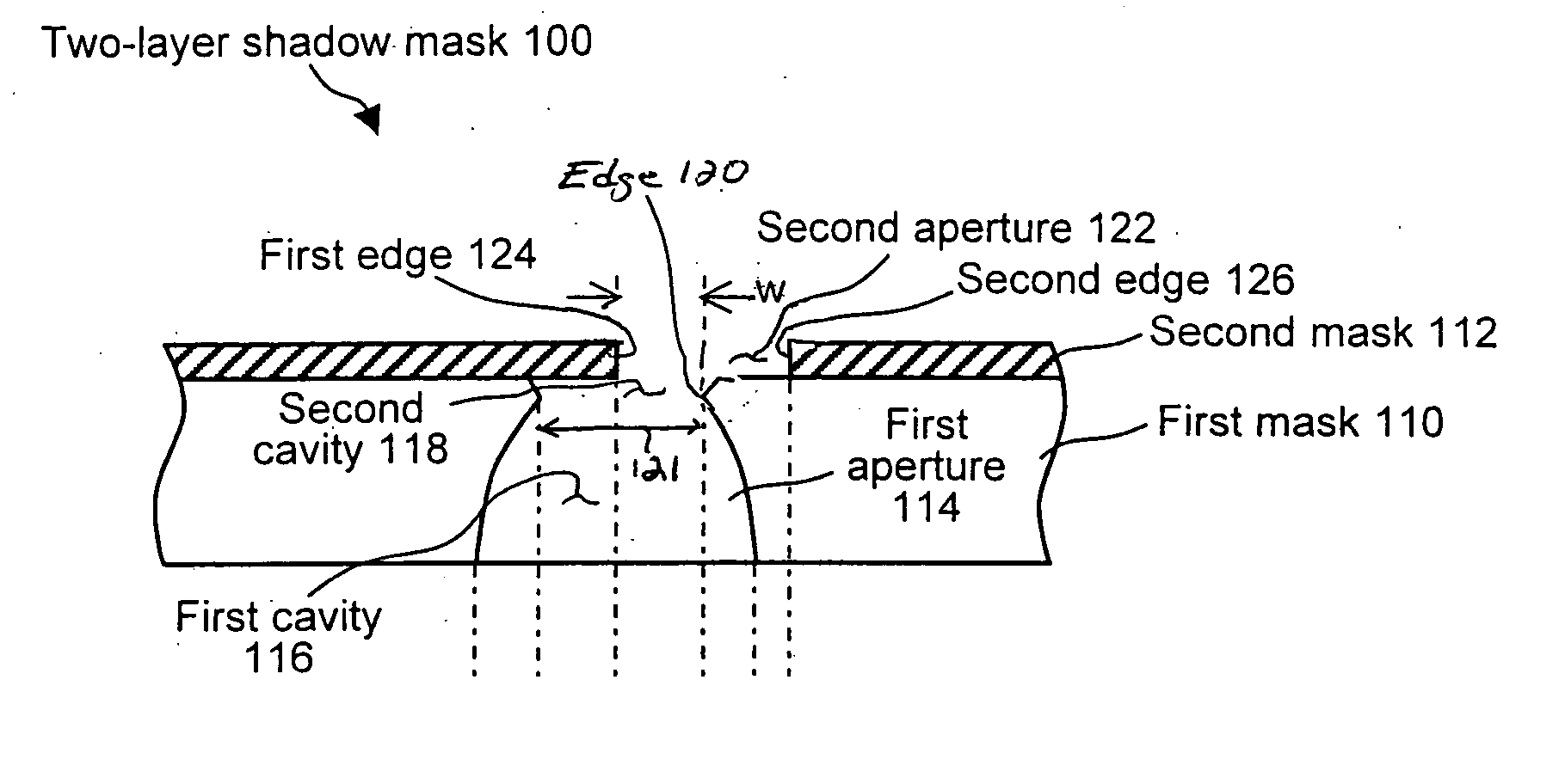
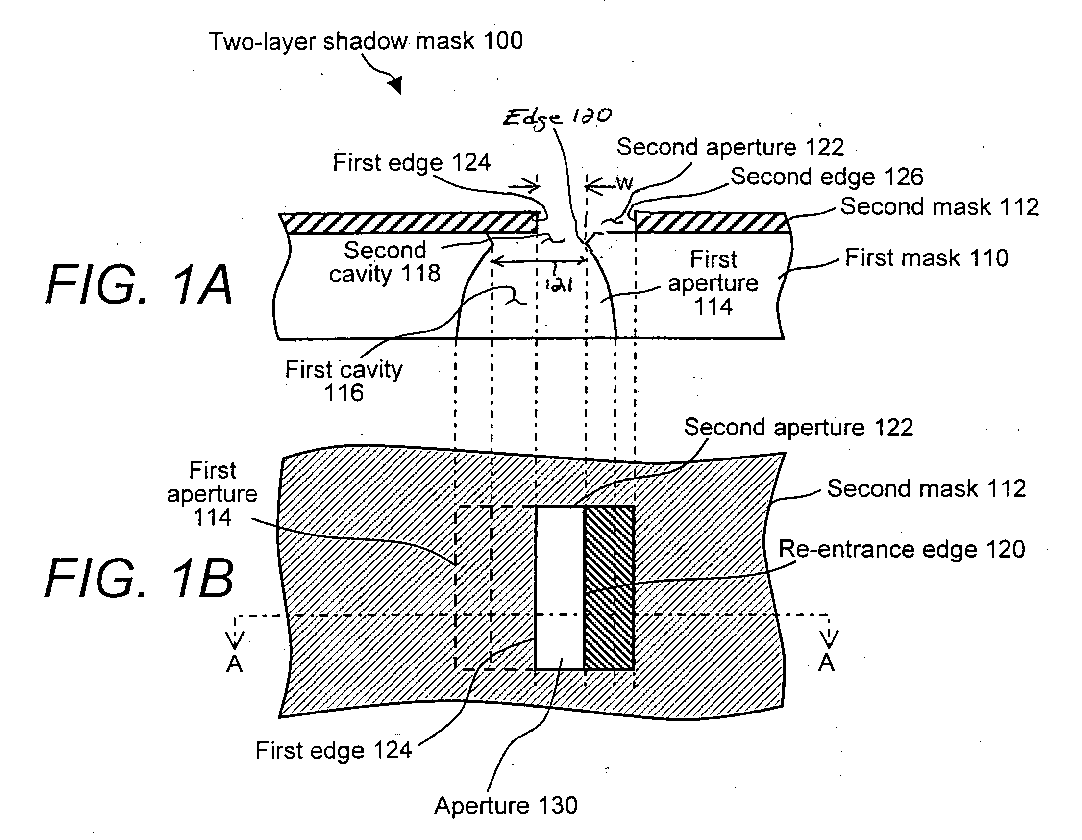
[0033]FIG. 1A illustrates a cross-sectional view of a two-layer shadow mask 100 taken along line A-A of FIG. 1B, which is a top view of the same in accordance with the invention. Two-layer shadow mask 100 is suitable for use in a production system, such as a standard vapor deposition process in a vacuum chamber, for manufacturing an electronic device and provides a smaller dimensioned aperture than a conventional single-layer shadow mask.

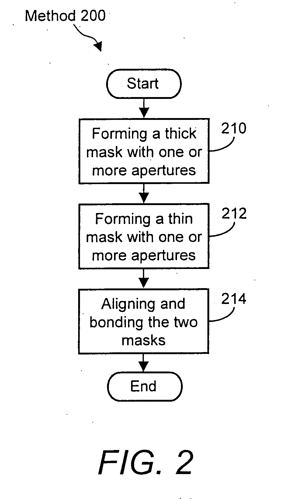
[0034] Two-layer shadow mask 100 includes a first layer or mask 110 formed of, for example, nickel, chromium, steel, or copper, having a thickness of, for example, 150-200 microns. First mask 110 of two-layer shadow mask 100 is bonded to a thinner, second layer or mask 112 that is formed of, for example, nickel via an electroformed nickel process, and that has a minimum thickness of, for example, 10 microns. To form two-layer shadow mask 100, first mask 110 and second mask 112 are joined together by well-known techniques, such as, without limitatio...


PUM

PropertyMeasurementUnit
thicknessaaaaaaaaaa
thicknessaaaaaaaaaa
widthaaaaaaaaaa

Abstract

The present invention is a two-layer shadow mask with small dimension apertures and method of making and using same. The two-layer shadow mask of the present invention is suitable for use for manufacturing an electronic device via deposition in a production system. The two-layer shadow mask of the present invention is formed by a first thick mask, which includes a plurality of apertures that has been formed, for example, by etching, bonded to a second, comparatively thin mask, that has been formed by an electrolytic process, and which includes a plurality of apertures that has been patterned by a photoresist. The second mask is aligned and bonded atop the first mask, with their respective apertures desirably offset one to another. The offset amount of the respective apertures of the two-layer shadow mask determines the resulting final aperture dimension, which may approach 0 microns, through which material is deposited upon a substrate in a deposition production system.

Description

BACKGROUND OF THE INVENTION [0001] 1. Field of the Invention [0002] The present invention relates to a shadow mask and, more particularly, to a two-layer shadow mask for forming electronic elements on a substrate. [0003] 2. Description of Related Art [0004] Active matrix backplanes are widely used in flat panel displays for routing signals to pixels of the display in order to produce viewable pictures. Presently, active matrix backplanes for flat panel displays are formed by a photolithography manufacturing process, which has been driven in the market by the demand for higher and higher resolution displays, which is not otherwise possible with other manufacturing processes. Photolithography is a pattern definition technique which uses electromagnetic radiation, such as ultraviolet (UV) radiation, to expose a layer of resist that is deposited on the surface of a substrate. Exemplary photolithography processing steps to produce an active matrix backplane include coat photoresist, pre-...

Claims


Application Information

Patent Timeline
Patent Type & Authority Applications(United States)
IPC IPC(8): B05D1/32B05C11/11B05D1/40
CPCC23C14/042H01L51/0011C23C14/562H10K71/166
Inventor BRODY, THOMAS PETER
Owner ADVANTECH GLOBAL LTD
Features
  • R&D
  • Intellectual Property
  • Life Sciences
  • Materials
  • Tech Scout
  • Unparalleled Data Quality
  • Higher Quality Content
  • 60% Fewer Hallucinations
Learn More