Storage device system and signal transmission method for storage device system

a storage device and signal transmission technology, applied in the field of storage device systems, can solve the problems of degrading signal quality, increasing the dielectric loss of printed circuit boards, and affecting the signal quality, so as to and prevent the degradation of signal quality

Inactive Publication Date: 2006-02-02
HITACHI LTD
View PDF14 Cites 15 Cited by
  • Summary
  • Abstract
  • Description
  • Claims
  • Application Information

AI Technical Summary

Benefits of technology

[0011] Therefore, it is an object of the present invention to prevent degradation of signal quality during transmission from or to a plurality of storage devices. More specifically, for example, one object of the present invention is to prevent degradation of signal quality during transmission from or to a plurality of storage devices using high-speed serial transfer, where dielectric loss is the dominant factor in signal degradation. It is also an object of the present invention to prevent degradation of signal quality during transmission to or from storage devices, even if the plurality of storage devices include storage devices having a transmission path which exceeds a prescribed length. It is also an object of the present invention to prevent degradation of signal quality during transmission to or from a plurality of storage devices having different storage device attributes (for example, at least one attribute out of the data transfer speed, the device type and the device provider).

Problems solved by technology

If it is supposed that HDDs capable of performing serial data transfer at high speeds of this kind are installed in a disk array device, and that the control device and the HDDs are connected via one or more printed circuit boards, then signal loss can be envisaged due to one or more than one problem, such as signal loss caused by the skin effect of the printed circuit boards or by dielectric loss, or signal loss caused by impedance mismatching of the interface connectors which connect the printed circuit boards with the HDDs.
It is thought that the increase in dielectric loss in the printed circuit board becomes particularly problematic, if the transmission frequency exceeds 1 GHz in the signal path through the printed circuit board (for example, if the transmission frequency is 2 GHz or above).
This is because if the dielectric loss increases, then the leakage current also increases, thus degrading the signal quality.
Consequently, degradation of signal quality is expected to be a problem if an HDD capable of high-speed serial data transfer is installed in a disk array device.
Therefore, deterioration of the signal quality due to transmission loss is also thought to be a potential problem.

Method used


Image

  • Storage device system and signal transmission method for storage device system
  • Storage device system and signal transmission method for storage device system
  • Storage device system and signal transmission method for storage device system

Examples


embodiment 1

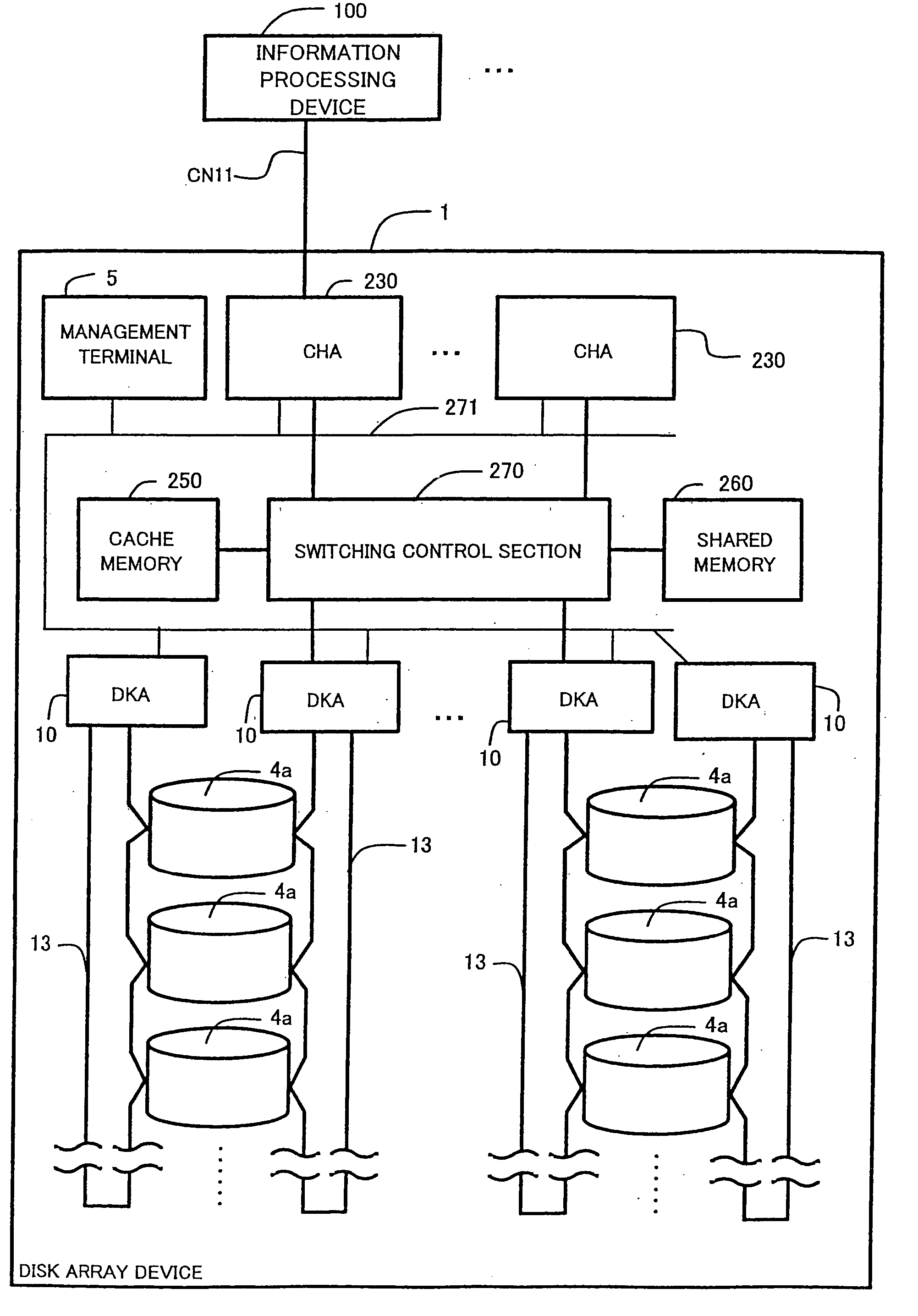
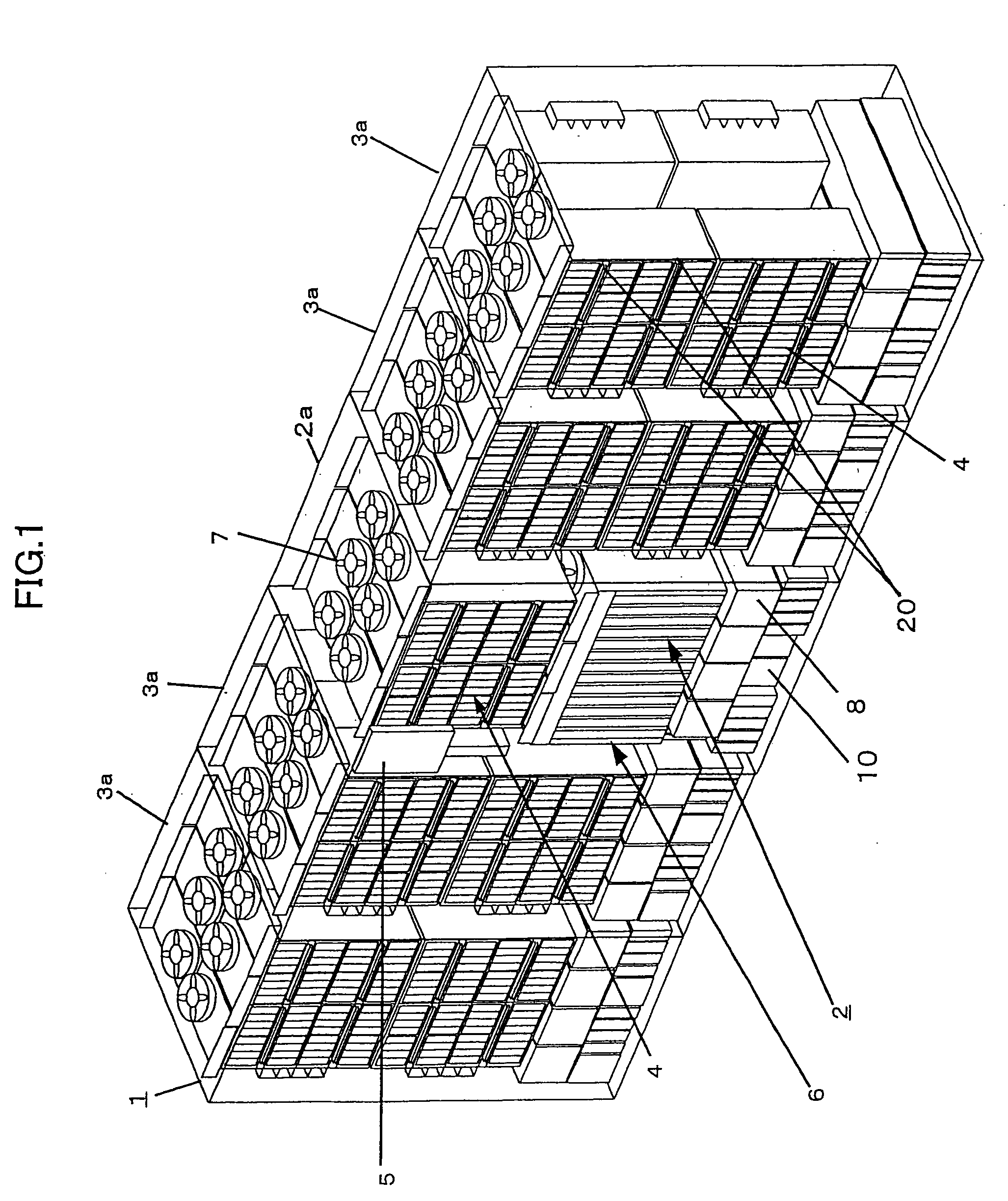
[0067]FIG. 1 shows an external view of the general composition of a disk array device relating to a first embodiment of one mode of implementing the present invention.

[0068] The disk array device 1 comprises a controller frame 2a capable of accommodating a disk control device 2 and a canister 4 in a central position, and disk drive frames 3a capable of accommodating canisters 4, to the left and right-hand sides of the controller frame 2a. The canisters 4 contain disk drives. For the disk drives, it is possible to use various types of device, such as a hard disk drive (HDD), or a semiconductor storage device, or the like. The controller frame 2a corresponds to the basic frame and the disk drive frames 3a are so-called expansion frames, which may not be provided at all, or which may be provided in plural fashion.

[0069] The control frame 2a controls the disk array device 1. The control frame 2a comprises, for example, a management terminal 5, a disk control device 2, cooling fans 7, ...

embodiment 2

[0181] Next, a second embodiment of the first mode of implementing the present invention will be described. The following description will focus on differences with respect to the first embodiment, and points which are common with the first embodiment are either omitted or are explained briefly.

[0182]FIG. 24 shows an example of the composition of an HDD control board 20 according to the second embodiment of the present invention.

[0183] In the signal correction value table 805, a plurality of wavelength attributes are registered for respective disk drive installation positions, and boost values are registered for each of the wavelength attributes. Here, “wavelength attribute” means information relating to the wavelength of the transmitted data, for example, the data pattern.

[0184] The board control section 815 reads out information from the signal correction value table 805 and registers it in the boost value setting region 817, and the information registered in the boost value se...

third embodiment

[0188]FIG. 25A shows an example of the composition of a canister relating to a third embodiment of the first mode of implementing the present invention. FIG. 25B is a block diagram of the canister 4 shown in FIG. 25A.

[0189] The canister is provided with a DC / DC connector 887, and a circuit board 891 comprising a DC / DC converter 893.

[0190] The DC / DC connector 887 is connected to the DC / DC converter 893, and it also connects to a DC / DC connector 888 provided on the back plane board 22. If the DC / DC connector 887 is connected to the DC / DC connector 888 of the back plane board 22 (in other words, if it is powered up), then a disk identification signal, described hereinafter (for example, a signal wherein only one prescribed bit of an 8-bit signal is set to high level) is output to the circuit board 891.

[0191] The DC / DC converter 893 converts the DC voltage supplied via the DC / DC connector 887 (for example, 48V), into a DC voltage corresponding to the disk drive 4a (for example, 5V or...


PUM

PropertyMeasurementUnit
frequencyaaaaaaaaaa
transmission frequencyaaaaaaaaaa

Abstract

The storage device system comprises: a plurality of signal transmission paths connected respectively to a plurality of installed storage devices; a plurality of system side communications sections for transmitting and receiving signals respectively to and from the plurality of storage devices, via the plurality of signal transmission paths; and one or a plurality of signal correcting sections for inputting a signal exchanged between the plurality of storage devices and the plurality of system side communications sections, correcting the input signal on the basis of a previously established correction parameter, and outputting the corrected signal. The correction parameter is a value set on the basis of at least one of the length of the signal transmission path between the storage device and the system side communications section, the wavelength attribute of the signal input to the signal correcting section, and the storage device attribute relating to the storage device.

Description

CROSS-REFERENCE TO PRIOR APPLICATION [0001] This application relates to and claims priority from Japanese Patent Application Nos. 2004-222031, filed on Jul. 29, 2004 the entire disclosure of which is incorporated herein by reference. FIELD OF THE INVENTION [0002] The present invention relates to a storage device system, and more particularly, to a technology for transmitting signals to a plurality of storage devices installed in a storage device system. BACKGROUND OF THE INVENTION [0003] For example, as disclosed in Japanese Patent Laid-open No. 2000-347816, a disk array device provided with a fiber channel loop, a control device and a plurality of disk devices is known. The control device and the plurality of disk devices are connected to the fiber channel loop. The control device accesses any one of the plurality of disk devices, via the fiber channel loop. SUMMARY OF THE INVENTION [0004] It is known that in a FC-AL (Fiber Channel Arbitrated Loop), communications can be conducted ...

Claims


Application Information

Patent Timeline
Patent Type & Authority Applications(United States)
IPC IPC(8): G06F12/14G06F13/00G06F12/16G06F12/00G06F13/28G06F3/00G06F3/06G11B20/10H04B3/04H04L25/03
CPCH04L25/03343G06F13/4072
Inventor MATSUSHIGE, HIROMISUZUKI, HIROSHIOGAWA, MASATO
Owner HITACHI LTD
Why Eureka
Try Eureka