Semiconductor integrated circuit device

a technology of integrated circuits and semiconductors, applied in electronic switching, pulse techniques, instruments, etc., can solve the problem of inability to reduce the voltage loss in normal operation, and achieve the effect of reducing the on-state resistance of the second mos transistor and reducing the voltage loss

Active Publication Date: 2006-02-09
ROHM CO LTD
View PDF6 Cites 3 Cited by
  • Summary
  • Abstract
  • Description
  • Claims
  • Application Information

AI Technical Summary

Benefits of technology

[0011] An object of the present invention is to provide a semiconductor integrated circuit device that can prevent a backflow current and that operates with low voltage loss in normal operation.
[0013] In this configuration, in a reversely-biased state, i.e., when the first direct-current voltage is lower than the second direct-current voltage, the second MOS transistor turns off, and this prevents a backflow current in the first MOS transistor. On the other hand, in normal operation, i.e., when the first direct-current voltage is higher than the second direct-current voltage, the gate of the second MOS transistor is connected to the predetermined potential, and this makes it possible to reduce the on-state resistance of the second MOS transistor. Thus, it is possible to reduce the voltage loss in normal operation. Here, the on-state resistance of the second MOS transistor is at its minimum when the gate thereof is connected to ground, and therefore, in normal operation, i.e., when the first direct-current voltage is higher than the second direct-current voltage, it is preferable that the gate of the second MOS transistor be connected to ground.
[0014] By using MOS transistors of the same conductivity as the first and second MOS transistors, it is possible to prevent, by the action of the parasitic diode formed within the second MOS transistor, the backflow current caused by the parasitic diode formed within the first MOS transistor. Since a P-channel MOS transistor can be formed in a smaller size than an N-channel MOS transistor, it is preferable to use P-channel MOS transistors as both the first and second MOS transistors.

Problems solved by technology

This makes it impossible to reduce the voltage loss in normal operation.
This makes it impossible, in a case where the on-state resistance of the power supply shut-off switch is high, to reduce the voltage loss in normal operation (the operation performed when the external supply voltage is higher than a predetermined level).

Method used


Image

  • Semiconductor integrated circuit device
  • Semiconductor integrated circuit device
  • Semiconductor integrated circuit device

Examples


Embodiment Construction

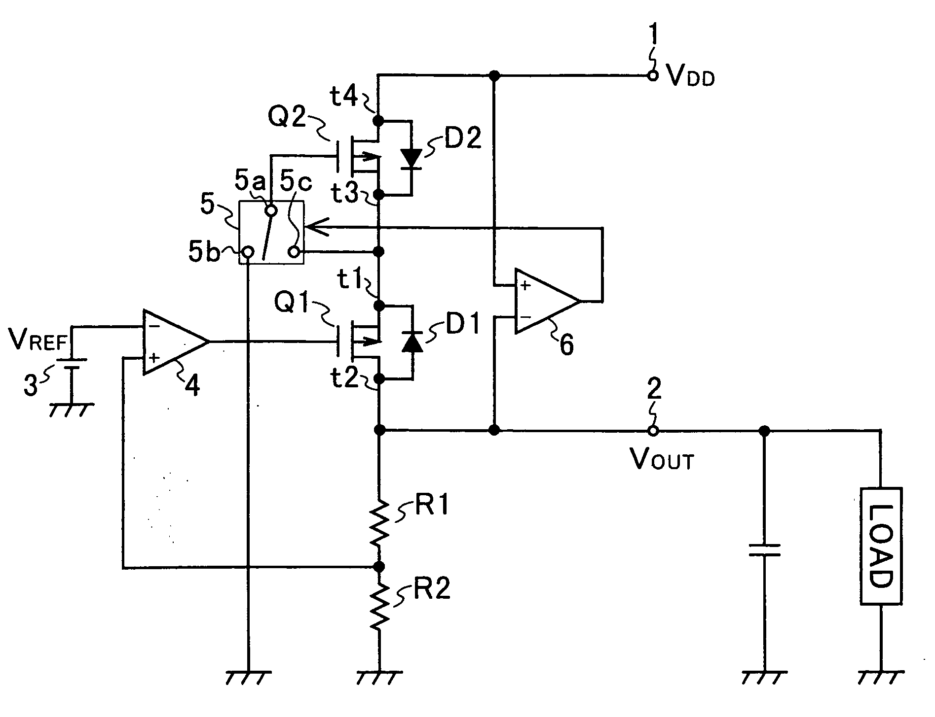
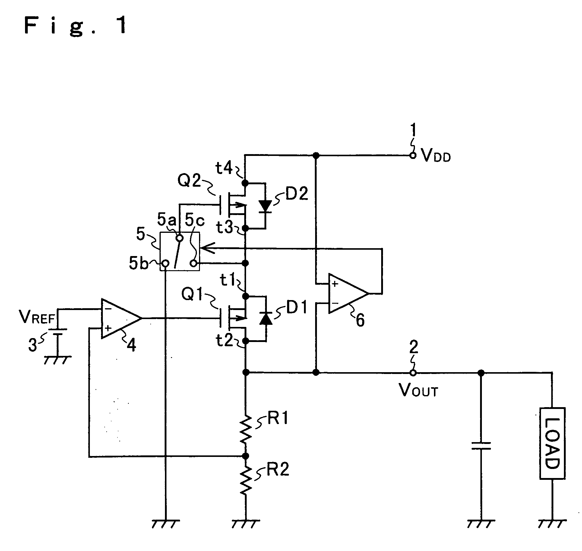
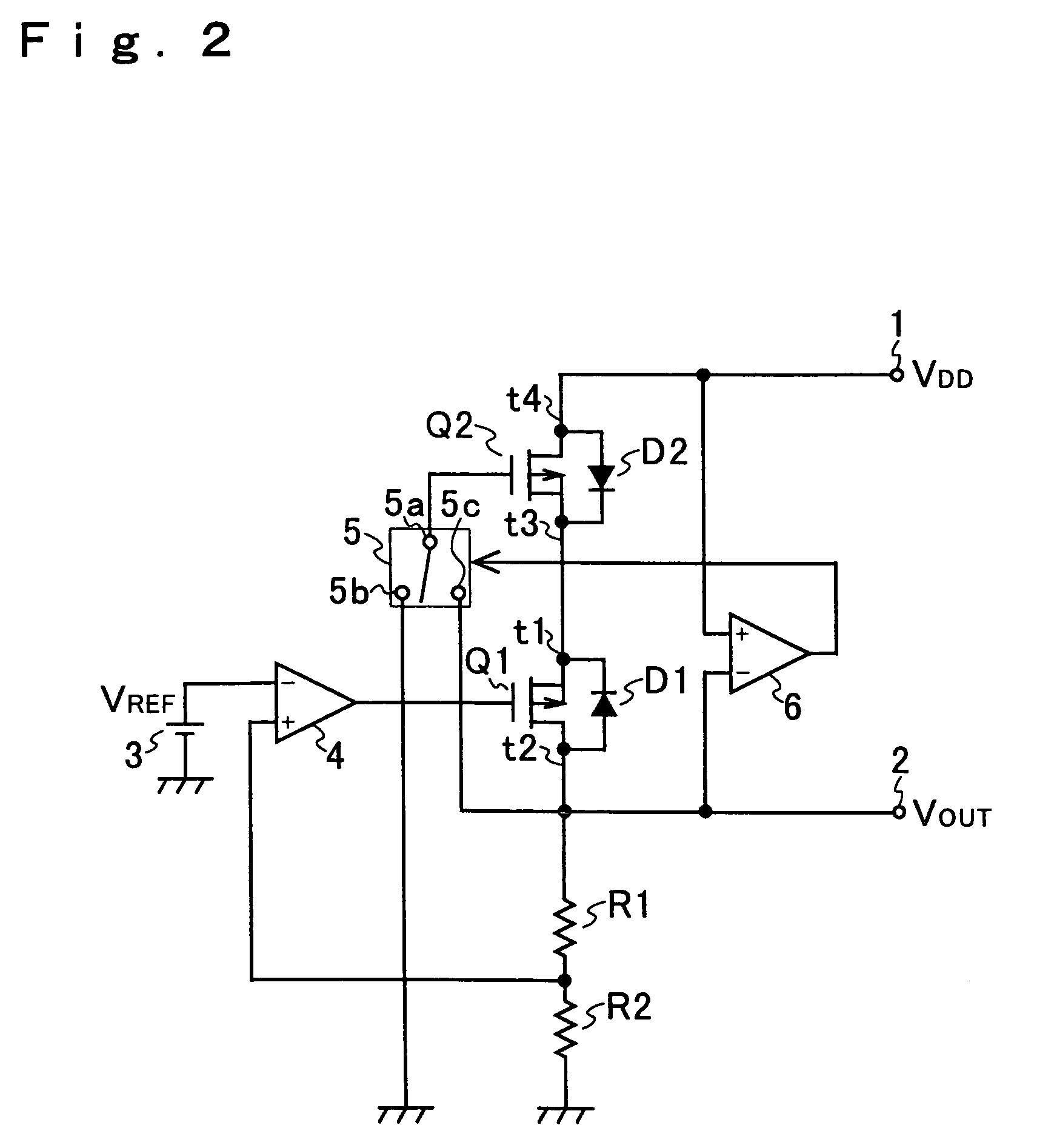
[0021] As an example of a semiconductor integrated circuit device embodying the invention, a regulator will be described below. FIG. 1 shows an example of the configuration of a regulator embodying the invention. It should be noted that, in FIG. 1, such circuit elements as are found also in FIG. 5 are identified with the same reference numerals, and their detailed explanations will not be repeated.

[0022] The regulator shown in FIG. 1 is provided with a power supply terminal 1, an output terminal 2, a reference voltage source 3, an error amplifier 4, a switch 5, a comparator 6, P-channel MOS transistors Q1 and Q2, and resistors R1 and R2.

[0023] Between the power supply terminal 1 and the output terminal 2, the MOS transistors Q1 and Q2 are connected in series. Specifically, the power supply terminal 1 is connected to the conducting terminal t4 of the MOS transistor Q2; the backgate and conducting terminal t3 of the MOS transistor Q2 is connected to the conducting terminal t1 and ba...


PUM


Abstract

In a conventional semiconductor integrated circuit device, a means for preventing a backflow current has a high on-state resistance, which makes it impossible to reduce the voltage loss in normal operation. A semiconductor integrated circuit device of the invention has a first MOS transistor, a second MOS transistor provided between the first MOS transistor and a power supply terminal, and a means that, in normal operation, keeps the gate of the second MOS transistor at a predetermined potential (preferably the ground potential) and that, when a backflow current is likely, turns the second MOS transistor off. This helps prevent a backflow current while reducing the voltage loss in normal operation.

Description

[0001] This is a divisional application which claims the benefit of pending U.S. patent application Ser. No. 10 / 814,248, filed Apr. 1, 2004, which is based on Japanese Patent Application No. 2003-101366 filed on Apr. 4, 2003. The disclosures of the prior applications are hereby incorporated in their entirety by reference.BACKGROUND OF THE INVENTION [0002] 1. Field of the Invention [0003] The present invention relates to a semiconductor integrated circuit device having a MOS transistor. More particularly, the present invention relates to a semiconductor integrated circuit device provided with a means for preventing a backflow current in a MOS transistor. [0004] 2. Description of the Prior Art [0005] Some semiconductor integrated circuit devices incorporate a P-channel MOS transistor Q5 having a supply voltage VDD applied to the source and backgate thereof as shown in FIG. 4. In this MOS transistor Q5, a parasitic diode D5 is formed from the drain to the backgate. [0006] As a result, ...

Claims


Application Information

Patent Timeline
Patent Type & Authority Applications(United States)
IPC IPC(8): G05F1/10H03K17/06G05F1/56H03K17/0814H03K17/14H03K17/687
CPCG05F1/56H03K17/145H03K17/08142H03K17/687
Inventor KONDO, MASAHITOINOUE, KOICHI
Owner ROHM CO LTD
Why Eureka
Try Eureka