Electrostatic discharge protection for an integrated circuit

a technology of integrated circuits and electrostatic discharge, which is applied in the direction of diodes, semiconductor devices, electrical apparatus, etc., can solve the problems of far too resistive parametric sti diodes to provide robust esd protection

Inactive Publication Date: 2006-02-09
FREESCALE SEMICON INC
View PDF10 Cites 38 Cited by
  • Summary
  • Abstract
  • Description
  • Claims
  • Application Information

AI Technical Summary

Problems solved by technology

However, in many typical output buffer physical layouts, these parasitic STI diodes are far too resistive to provide robust ESD protection.

Method used


Image

  • Electrostatic discharge protection for an integrated circuit
  • Electrostatic discharge protection for an integrated circuit
  • Electrostatic discharge protection for an integrated circuit

Examples


Embodiment Construction

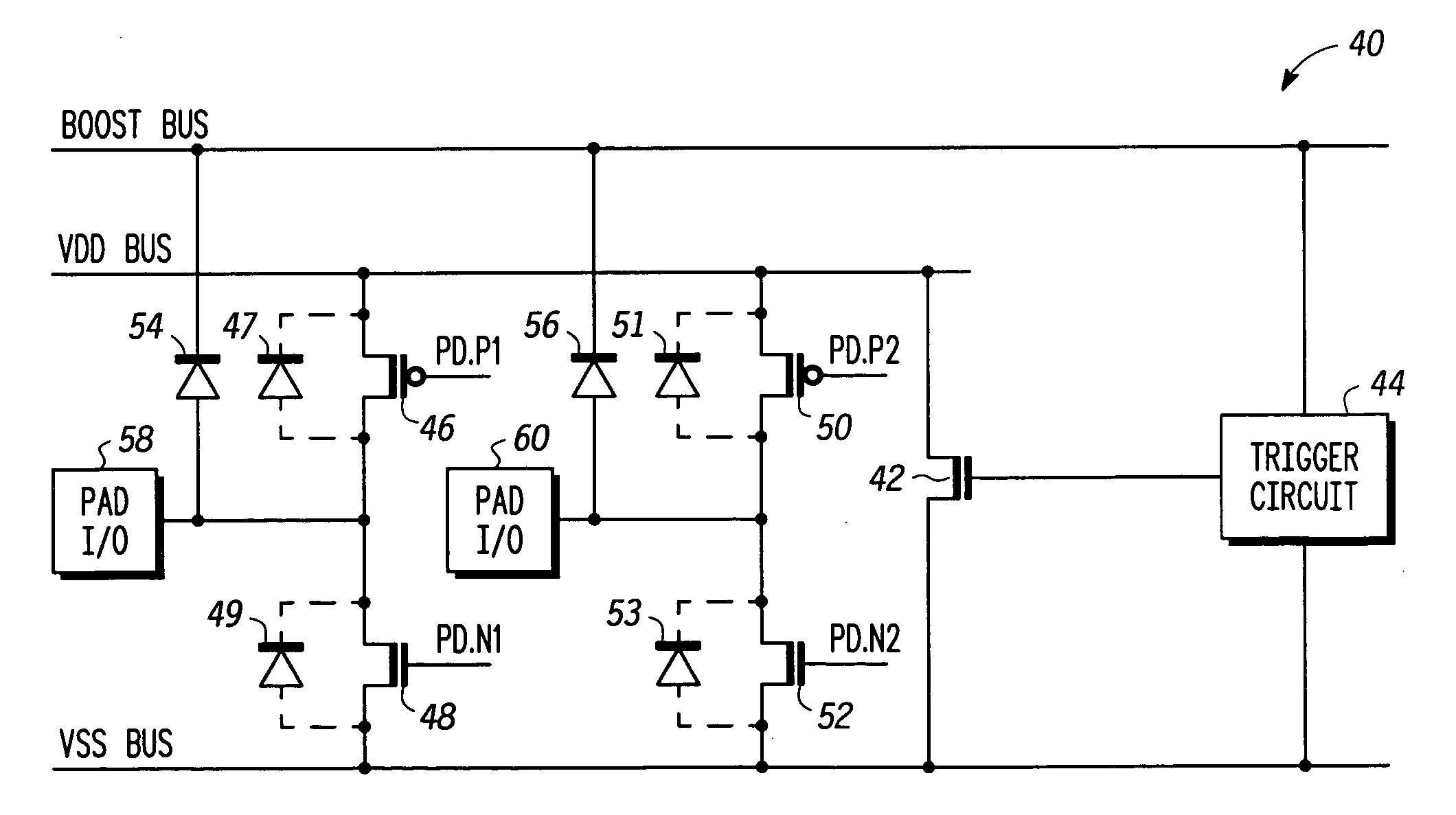
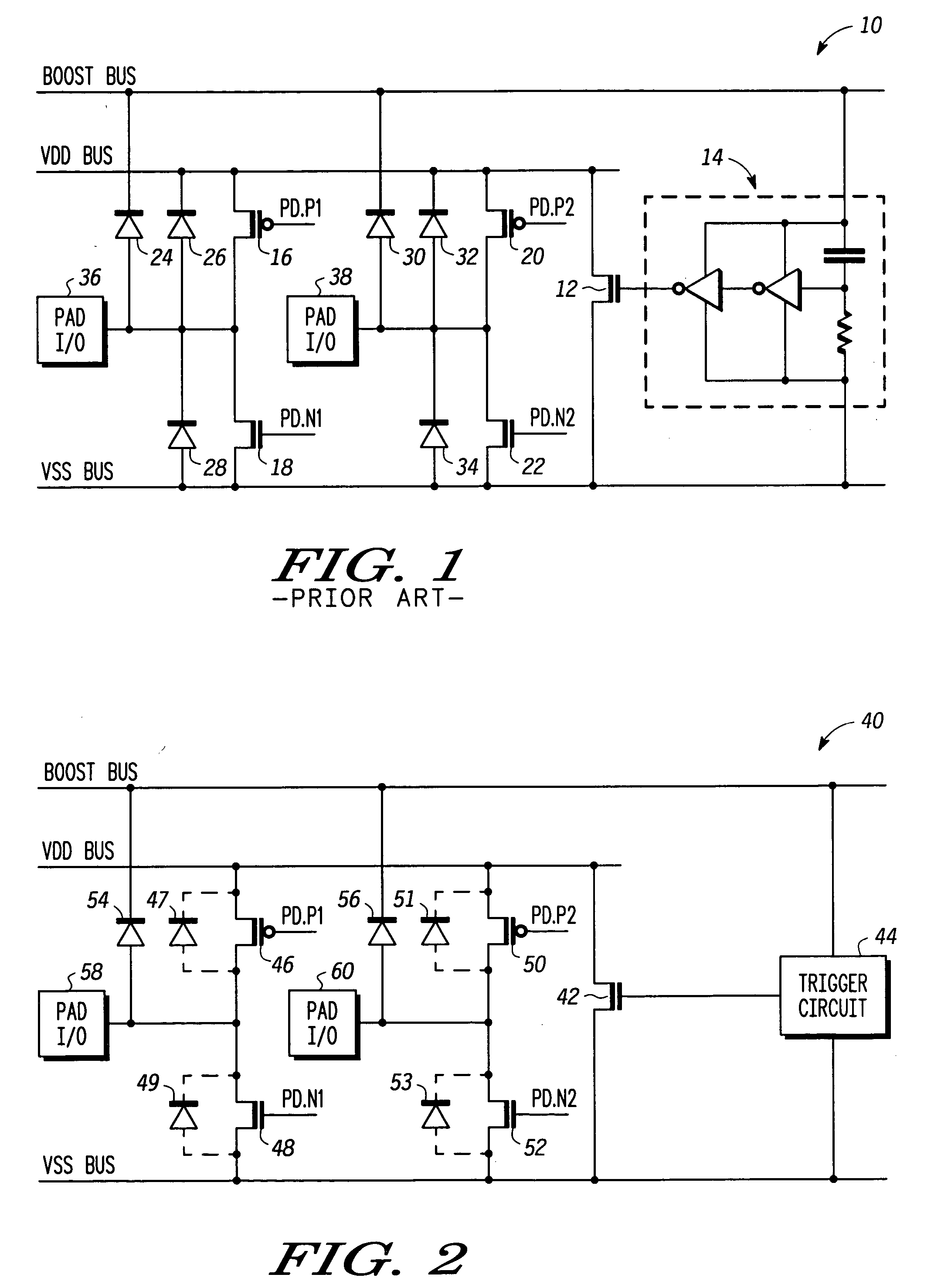
[0014] Generally, the present invention provides an ESD protection circuit for the I / O pad cells of an IC. The ESD protection circuit uses parasitic drain-body diodes of the output buffer transistors as the primary, or dominant, ESD diodes. Specifically, the body tie diffusions of the output buffer transistors are butted to the source diffusions without an isolation region (STI) between the two diffusion regions (“butted source-body ties”). Utilizing parasitic drain-body diodes of output buffer transistors with butted source-body ties (“butted body tie diodes”) as the dominant ESD diodes eliminates the layout area required to implement separately placed STI diodes of the prior art circuit of FIG. 1.

[0015]FIG. 2 illustrates in schematic diagram form an ESD protection circuit 40 in accordance with one embodiment of the present invention. ESD protection circuit 40 includes a first power supply bus labeled “VDD BUS”, a second power supply bus labeled “VSS BUS”, and a boosted voltage bu...


PUM


Abstract

An ESD protection circuit (40) uses parasitic drain-body diodes (47, 49) of the output buffer transistors (46, 48) as the main, or dominant, ESD protection diodes. Specifically, butted source-body ties in the output buffer transistors (46, 48) provide the ESD diodes (47, 49). Using parasitic drain-body diodes of output buffer transistors with butted source-body ties as the dominant ESD diodes reduces the layout area required to implement the ESD protection circuit as compared to an ESD protection circuit having stand alone diodes. Also, the butted source-body ties reduce susceptibility to latch-up and reduce capacitive loading because there are no added diffusion regions tied to the pad.

Description

CROSS REFERENCE TO RELATED, COPENDING APPLICATIONS [0001] A related, copending application is entitled “Transient Detection Circuit”, Michael Stockinger et al., application Ser. No. 10 / 315,796, is assigned to the assignee hereof, and filed on Dec. 10, 2002. [0002] A related, copending application is entitled “Electrostatic Discharge Protection Circuit and Method of Operation”, Michael Stockinger et al., application Ser. No. 10 / 684,112, is assigned to the assignee hereof, and filed Oct. 10, 2003.FIELD OF THE INVENTION [0003] This invention relates generally to electrostatic discharge (ESD) protection for integrated circuits, and more specifically, to an ESD protection circuit that uses parasitic diodes as ESD protection devices. BACKGROUND OF THE INVENTION [0004] An integrated circuit (IC) may be subject to an Electrostatic Discharge (ESD) event in the manufacturing process, during assembly and testing, or in the system application. Some on-chip ESD protection networks use an active ...

Claims


Application Information

Patent Timeline
Patent Type & Authority Applications(United States)
IPC IPC(8): H02H9/00
CPCH01L27/0292H01L27/0255
Inventor STOCKINGER, MICHAELMILLER, JAMES W.
Owner FREESCALE SEMICON INC
Why Eureka
Try Eureka