High-power single-mode vertical cavity-surface emitting laser

a laser and vertical cavity technology, applied in semiconductor lasers, laser details, optical resonator shape and construction, etc., can solve the problems of device to generate more heat, low uniformity, low yield, etc., and achieve stable generation and restraint of high-level generating.

Inactive Publication Date: 2006-02-09
BENQ CORP
View PDF3 Cites 16 Cited by
  • Summary
  • Abstract
  • Description
  • Claims
  • Application Information

AI Technical Summary

Benefits of technology

[0010] The present invention can provide a surface emitting laser capable of being operated as an output single-mode laser. The single-mode surface emitting laser has an anti-reflection film, whose thickness is controlled, covering the top emitting region. Therefore, the anti-reflection film can restrain the high-level generating works so that the single-mode laser can be generated stably.

Problems solved by technology

Because the widths W1 and W2 are not easily controlled, the uniformity may be low and the yield may be low.
Furthermore, the whole device may have larger resistance (for example, hundreds of ohms), causing the device to generate more heat and potentially reducing the lighting power of the whole device by about 1 mW.
This seriously affects the device's life.

Method used


Image

  • High-power single-mode vertical cavity-surface emitting laser
  • High-power single-mode vertical cavity-surface emitting laser
  • High-power single-mode vertical cavity-surface emitting laser

Examples


first embodiment

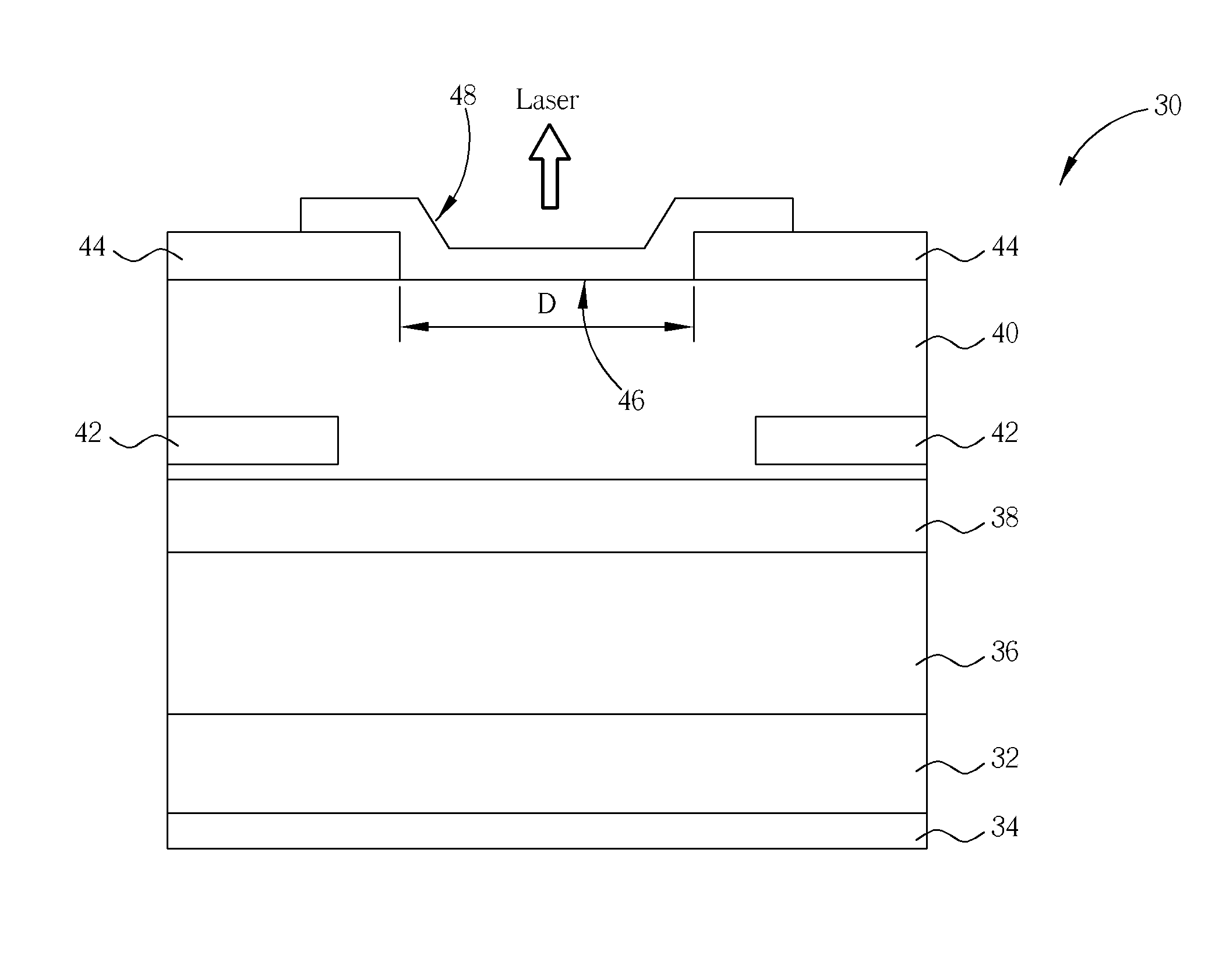
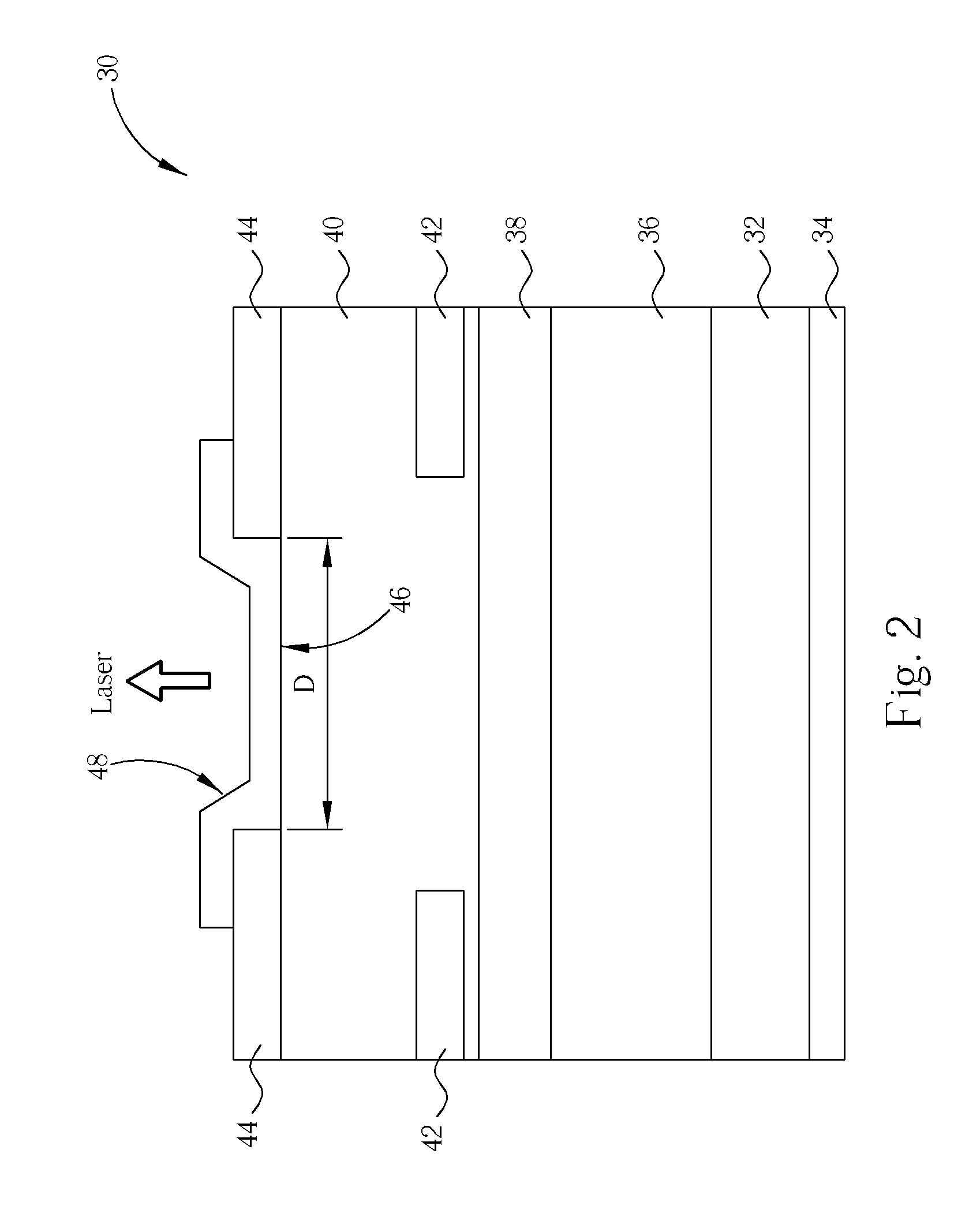
[0020] Please refer to FIG. 2, which is a diagram of a vertical cavity-surface emitting laser 30 capable of outputting single-mode lasers according to the present invention. In this embodiment, the vertical cavity-surface emitting laser 30 is produced through an ion-implanted technique. The vertical cavity-surface emitting laser 30 comprises a substrate 32; an N-type metal 34, which can comprise AuGe, Ni, and Au and is formed below the substrate 32; an N-type DBR 36, which can comprise compound semiconductor materials and is formed above the substrate 32; an active region 38 formed above the N-type DBR 36 for generating a laser; a P-type DBR 40, which can comprise compound semiconductor materials and is formed above the active region 38; an ion-implantation layer 42, which is formed in the P-type DBR 40 by doping and implanting protons whose density is 3*1014 ions / cm2 and whose energy is 300 KeV for limiting a flow direction of the injected currents of the vertical cavity-surface em...

third embodiment

[0028] Please refer to FIG. 5, which is a diagram of a vertical cavity-surface emitting laser 60 capable of outputting single-mode lasers according to the present invention. In this embodiment, the devices of the same number have the same function and structure, and are thus omitted here. In this embodiment, the VCSEL 60 is produced through the intracavity oxide-confined procedures. Therefore, the VCSEL 60 can be utilized in a high frequency device (e.g. >5 Gbps) or a range of visible lights and long wavelength. The VCSEL 60 also comprises a substrate 32; an N-type DBR 36, which can comprise compound semiconductor materials and is formed above the substrate 32; an N-type contact layer 62 which can comprise AuGe, Ni, and Au and is formed above the N-type DBR 32; an N-type metal 64 which can comprise AuGe, Ni, and Au and is formed above the N-type contact layer 62; an active region 38 formed above the N-type DBR 36 for generating a laser; a P-type contact layer 66 formed above the act...


PUM


Abstract

A vertical cavity-surface emitting laser (VCSEL) for emitting a single-mode laser including a multiple transverse mode VCSEL includes a top emitting region, and a dielectric film covering the top emitting region of the multiple transverse mode VCSEL completely, in order to limit the multiple transverse mode VCSEL to emit the single-mode laser.

Description

BACKGROUND OF THE INVENTION [0001] 1. Field of the Invention [0002] The invention relates to a vertical cavity-surface emitting laser capable of outputting a high-power and stable single-mode laser, and more particularly, to a vertical cavity-surface emitting laser having an anti-reflection film covering the top emitting region. [0003] 2. Description of the Prior Art [0004] Because a vertical cavity-surface emitting laser has the advantages of low threshold currents, circle-symmetric light, small emitting angle and is easily produced, in recent years the vertical cavity-surface emitting laser has become a good light source. In real applications, vertical cavity-surface emitting lasers can be divided into two types according to the light frequencies; single-mode and multiple mode. In a short distance light-communication transmission (for example, 300-500 meters), the multiple mode vertical cavity-surface emitting laser is utilized because the signal decays very fast so the transmissi...

Claims


Application Information

Patent Timeline
Patent Type & Authority Applications(United States)
IPC IPC(8): H01S3/08
CPCH01S5/028H01S5/18308H01S5/18341H01S2301/166H01S5/18377H01S5/18394H01S5/18369
Inventor CHEN, CHIH-CHENG
Owner BENQ CORP
Why Eureka
Try Eureka