Programmable memory device with an improved redundancy structure

a memory device and redundancy structure technology, applied in the field of solid-state memories, can solve the problems of increasing the complexity of the whole device, increasing the required area of the control circuitry, and affecting so as to reduce the waste of occupied area in the chip, improve the performance of the memory device, and reduce the waste of occupied area

Active Publication Date: 2006-02-16
STMICROELECTRONICS SRL +1
View PDF9 Cites 35 Cited by
  • Summary
  • Abstract
  • Description
  • Claims
  • Application Information

AI Technical Summary

Benefits of technology

[0023] One embodiment of the present invention provides a memory device exploiting the redundancy of columns or rows, in which any comparison between a received memory address and a faulty memory address does not have to be carried out. Thus, the access time to a memory location and, thus, the performance of the memory device is improved. In addition, being the columns (or rows) of memory cells grouped into a number of sets each one associated with a predetermined redundancy column (or row), the managing of the redundancy is very simple, depending only on a logic value taken by a flag. Furthermore, with such a simple solution the waste of occupied area in a chip is greatly reduced.

Problems solved by technology

One of the main disadvantages of such solutions is a penalization on the access time of a memory location, depending on the time required to carry out the comparison between received memory addresses and all the faulty memory addresses stored in the additional memory.
Such a choice is very advantageous, but every increase of the corrective capability of the redundancy provokes an increase of the required area for its control circuitry, as well as an increase of the whole device complexity.

Method used


Image

  • Programmable memory device with an improved redundancy structure
  • Programmable memory device with an improved redundancy structure
  • Programmable memory device with an improved redundancy structure

Examples


Embodiment Construction

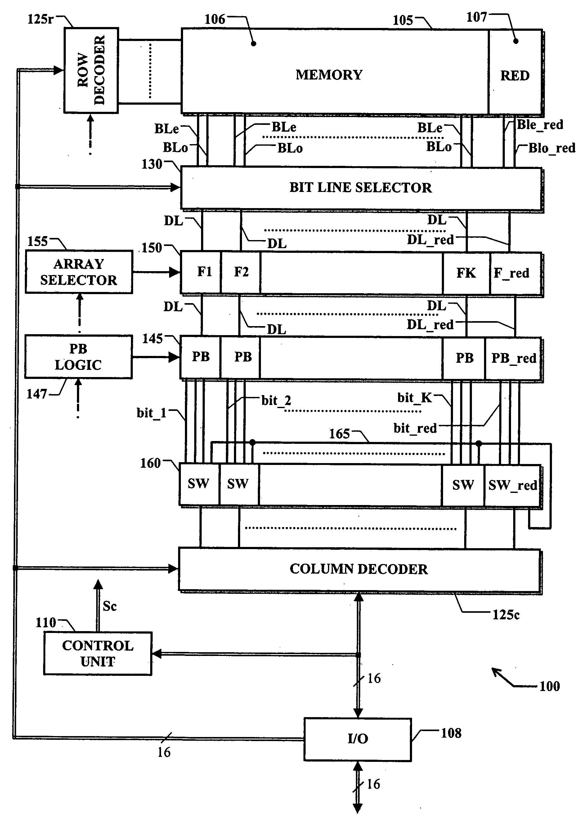
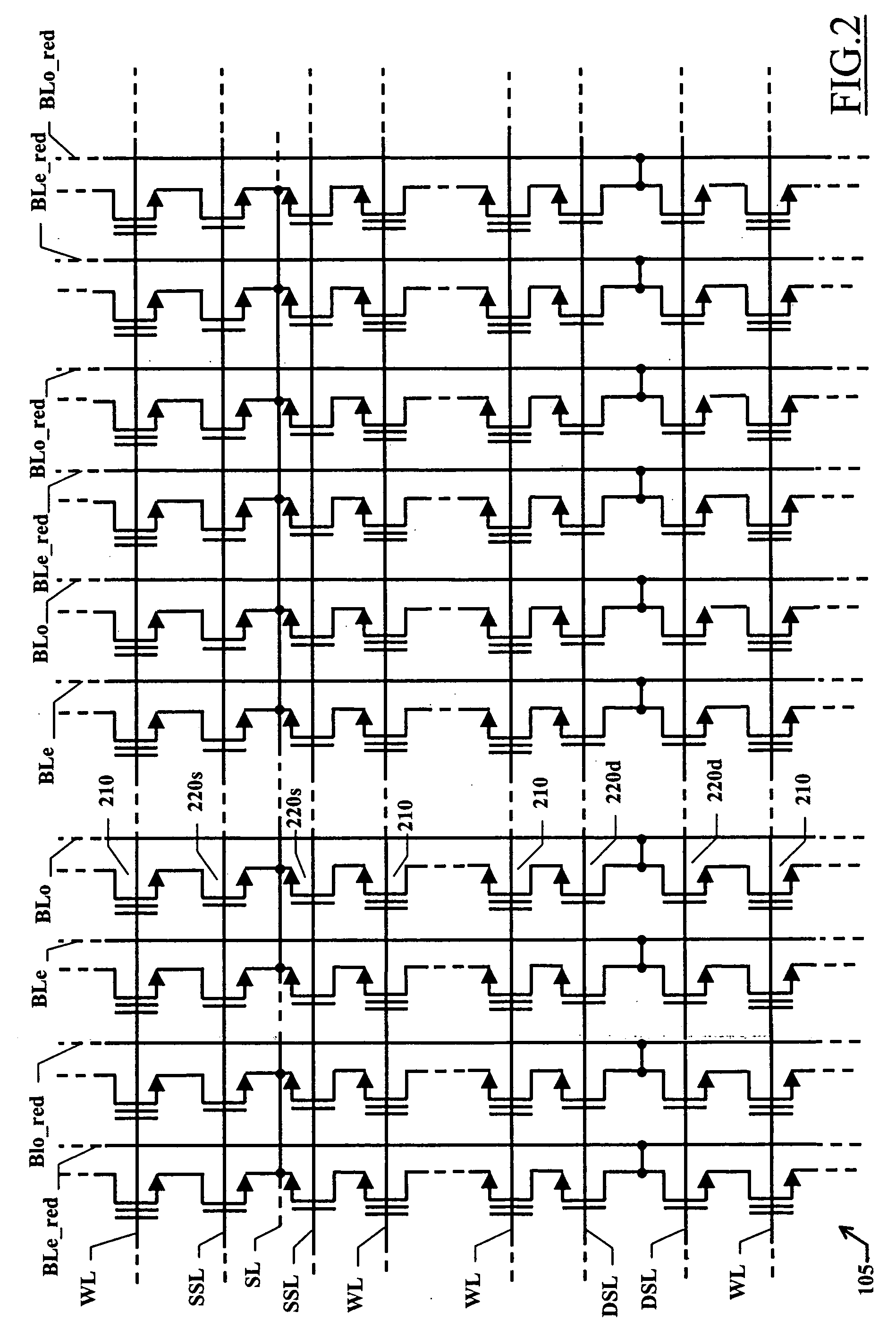
[0029] With reference to the drawings, FIG. 1 is a schematic block diagram of a memory device 100 according to an embodiment of the present invention, particularly an electrically-programmable, non-volatile memory, such as a flash memory. The flash memory 100 is integrated in a chip of semiconductor material and includes a matrix 105 of memory cells having a so-called NAND architecture (described in greater detail in the following).

[0030] The matrix of memory cells is logically partitioned into a memory portion 106 and a redundancy portion 107. The memory portion 106 includes a number Mc of columns of memory cells for storing data bits. The redundancy portion 107 includes a number Mr of redundancy columns of memory cells (hereinafter referred to as redundancy cells) for storing data bits in place of the memory cells of the memory portion 106 that are defective.

[0031] Each column of memory cells in even position is controlled by a corresponding bit line BLe, and each column of memo...


PUM


Abstract

An electrically programmable memory device is proposed including: a matrix of memory cells arranged in a plurality of memory arrays and at least one redundancy array; and a substituting structure that substitutes the use of each memory array with the use of one of the at least one redundancy array in response to a failure of the memory array, wherein the memory arrays are grouped into at least one set. The substituting structure includes: a structure for associating each set with a predetermined one of the at least one redundancy array; a flag for each memory array indicative of the failure of the memory array; and a selecting for enabling each memory array or the associated redundancy array according to the corresponding flag.

Description

BACKGROUND OF THE INVENTION [0001] 1. Field of the Invention [0002] The present invention generally relates to the field of solid-state memories, particularly to semiconductor memories and, even more particularly, to the field of non-volatile memories. Specifically, the invention relates to non-volatile memories that are electrically programmable. [0003] 2. Description of the Related Art [0004] Non-volatile memory devices are commonly used in several applications when the data stored in the memory device need to be preserved even when the power supply is off. Within the class of non-volatile memory devices, electrically programmable (and erasable) memory devices, such as flash memories, have become very popular in applications in which the data to be stored is not immutable (as it might be the case of, e.g., a consolidated code for a microprocessor), being instead necessary from time to time to store new data, or to update the data already stored. [0005] Typically, the memory device...

Claims


Application Information

Patent Timeline
Patent Type & Authority Applications(United States)
IPC IPC(8): G11C29/00
CPCG11C29/846
Inventor ZANARDI, STEFANO
Owner STMICROELECTRONICS SRL
Why Eureka
Try Eureka