Multiprocessor

a multi-processor and processor technology, applied in the field of multi-processors, can solve the problems of increasing the number of man-hours for development, serious problems, and increasing the frequency of debugging, and achieve the effect of high data transmission capacity and computation processing capacity

Inactive Publication Date: 2006-02-16
PANASONIC CORP
View PDF39 Cites 22 Cited by
  • Summary
  • Abstract
  • Description
  • Claims
  • Application Information

AI Technical Summary

Benefits of technology

[0032] For achieving the above object, the present invention can provide a multiprocessor having a high data transmission capacity and computation processing capacity as an entire system.

Problems solved by technology

Namely, since the circuit size in a semiconductor integrated circuit increases, an increase in the number of man-hours for development, an increase infrequency of debug, and the like raise serious problems.
There are cases where it is not inevitable to form all necessary parts as semiconductor integrated circuits, and in addition, if design and development is to be conducted on every occasion in response to upgrades of products, an increase in development cost and a delay of delivery of products tend to occur.
Furthermore, there are cases where the SoC cannot be packaged in a product in terms of costs.
Namely, in the SoC, functional blocks placed in one chip are interconnected by the internal data bus, and therefore data can be transferred at a high speed, while in the SiP, semiconductor chips within one package are interconnected via the wiring board, and therefore the data transfer speed is limited, thus inevitably decreasing the operation speed.
In this way, both the SoC and SiP have problems, and it is difficult in actuality to solve the problems.
However, the parallel computer system described above has a disadvantage that transmission between processors is retarded because a plurality of processors are coupled together.
Namely, the data transmission capacity of a data bus in the exterior of a semiconductor element (processor) is low compared with the data transmission capacity of a data bus in the interior of the semiconductor element (processor), and therefore this point is a bottleneck and the computation processing capacity cannot be fully exploited from a viewpoint of an entire system.
Namely, the system having a plurality of processors coupled together, such as the conventional parallel computer system, has a problem such that the computation processing capacity cannot be fully exploited as the entire system.

Method used


Image

  • Multiprocessor
  • Multiprocessor
  • Multiprocessor

Examples


embodiment 1

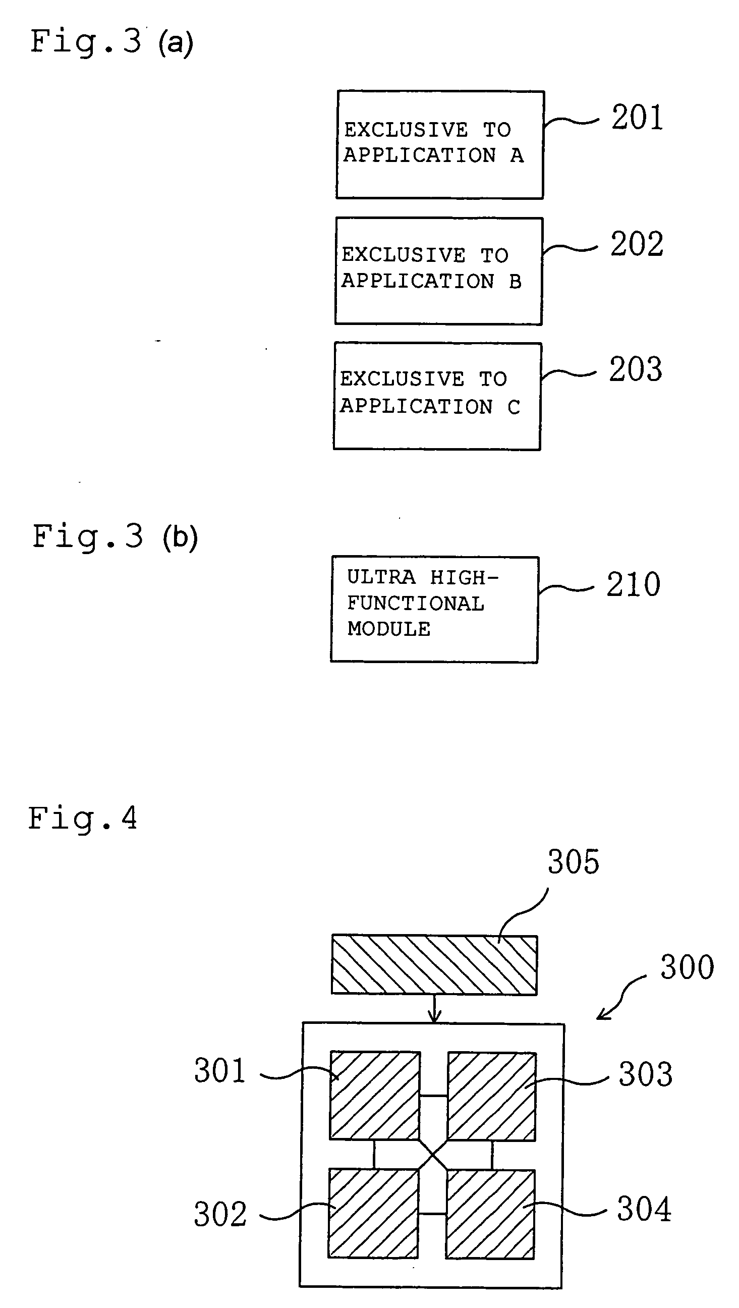
[0116] A computation circuit 300 according to the embodiment 1 of the present invention shown in FIG. 4 is constituted by a plurality of specific functional blocks 301, 302, 303 and 304. The specific functional blocks 301, 302, 303 and 304 are interconnected, and receive an instruction from a program portion (realized by software, a ROM or the like) 305 issuing an instruction to determine a combination according to various kinds of applications. According to the instruction from the program portion 305, the specific functional blocks 301, 302, 303 and 304 can dynamically change their combination.

[0117] For example, the computation circuit 300 operates with a combination of the specific functional blocks 301 and 302 for the application A, the computation circuit 300 operates with a combination of the specific functional blocks 303 and 304 for the application B, and the computation circuit 300 operates with a combination of the specific functional blocks 301, 302, 303 and 304 for the...

embodiment 2

[0201] The embodiment 2 of the present invention will now be described with reference to FIGS. 19 to 24. This embodiment mainly shows examples of application and examples of extension of the above-mentioned embodiment 1, and particularly shows that the technique of the embodiment of the present invention has a high degree of freedom and is rich in applicability and extensibility. For simplicity of explanation, aspects same as those of the above-mentioned embodiment 1 will be omitted.

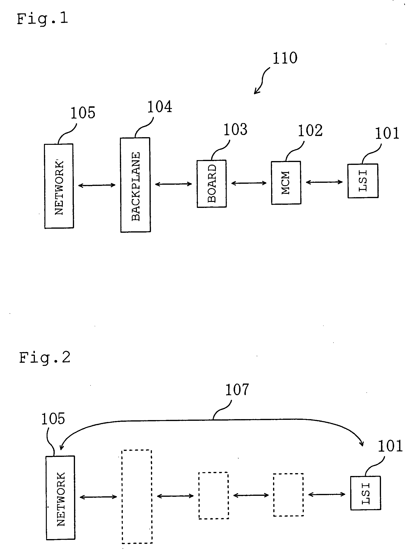
[0202] In the above-mentioned embodiment 1, a plurality of SiPs are placed exclusively in one product to construct the optical functional device 100, but the present invention is not limited thereto. If a plurality of SiPs are optically interconnected, an optical functional system as the optical functional device or a parallel computation system of this embodiment can be constructed even if departing from a form of one product. The example thereof is shown in FIG. 19.

[0203] In the configuration shown i...


PUM


Abstract

A parallel computation apparatus as a multiprocessor includes functional modules as a plurality of processors having an optical communication function and capable of mutually cooperating, and an optical transmission line interconnecting the plurality of processors. Among the plurality of functional modules, the first functional module having a first information processing capacity has a function of determining whether information processing of a first information processing amount can be completed based on the first information processing capacity, and outputting a second information processing amount obtained by subtracting an information processing amount based on the first information processing capacity from the first information processing amount to at least one of the other functional modules.

Description

BACKGROUND OF THE INVENTION [0001] 1. Field of the Invention [0002] The present invention relates to a multiprocessor which can be used as, for example, a parallel computation apparatus and an optical functional device. [0003] 2. Related Art of the Invention [0004] With miniaturization and enhancement of functions of electronic devices in recent years, attention has been given to a system-on-chip (SoC) realizing high-density and high-functional packaging using a system LSI in which a semiconductor device of one chip is equipped with a large number of functions (e.g. Japanese Patent Laid-Open No. 2003-188351). In the SoC, a plurality of functions are integrated into one chip with each thereof as a functional block, and functional blocks are interconnected by an internal data bus, and therefore the speed of operations can be enhanced by using the SoC. [0005] Use of the SoC offers various advantages such as an advantage that the speed of operations can be enhanced, while it brings abou...

Claims


Application Information

Patent Timeline
Patent Type & Authority Applications(United States)
IPC IPC(8): G06F12/10G06F9/34G06F15/00H04B10/27H04B10/272H04B10/80H04J14/00H04J14/02
CPCH04L12/00G06F15/16H04L49/109H04Q11/00G06F9/38
Inventor KARASHIMA, SEIJINAKATANI, SEIICHISAITO, YOSHIYUKI
Owner PANASONIC CORP
Why Eureka
Try Eureka