Method for designing an integrated circuit defect monitor

a defect monitor and integrated circuit technology, applied in the field of defect monitors, can solve the problems of increasing the difficulty of yield learning, the difficulty of defect monitor circuits and structures being inserted into integrated circuit chips, and the difficulty of ensuring the integrity of the integrated circuit, etc., to achieve the effect of reducing the cost of monitoring, increasing the size of the monitor structure, and increasing the difficulty of learning

Inactive Publication Date: 2006-02-16
IBM CORP
View PDF3 Cites 36 Cited by
  • Summary
  • Abstract
  • Description
  • Claims
  • Application Information

AI Technical Summary

Benefits of technology

[0006] A first aspect of the present invention is a method of designing a test structure, comprising: defining and placing test circuit pins in an integrated circuit design; routing one or more fat wires, each fat wire routed between a set of the test circuit pins; processing each fat wire into a continuous wire and one or more corresponding wire segments adjacent to the continuous wire, the continuous wire separated from the one or more corresponding wire segments by a space; and connecting the continuous wire and the one or more wire segments to circuit elements of a defect monitor scan chain, the circuit elements previously inserted into the integrated circuit design.
[0007] A second aspect of the present invention is a computer system comprising a processor, an address/data bus coupled to the proc...

Problems solved by technology

As integrated circuits have become more complex, yield learning has become more difficult and defect monitor circuits and structures have become increasing more difficult to insert into integrated circuit chips, especially application specific integrated circuit (ASIC) chips where chip area ...

Method used


Image

  • Method for designing an integrated circuit defect monitor
  • Method for designing an integrated circuit defect monitor
  • Method for designing an integrated circuit defect monitor

Examples


Embodiment Construction

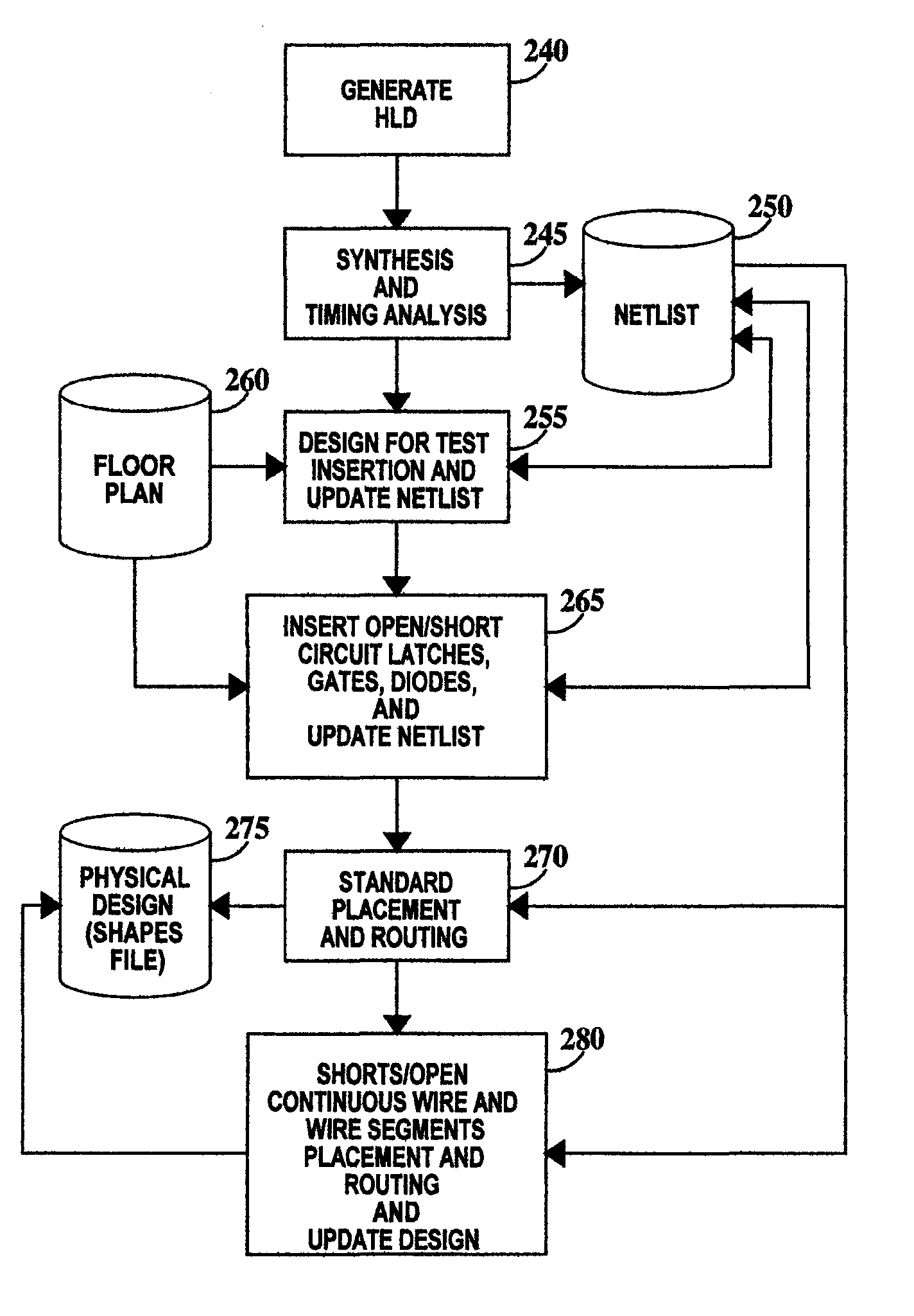
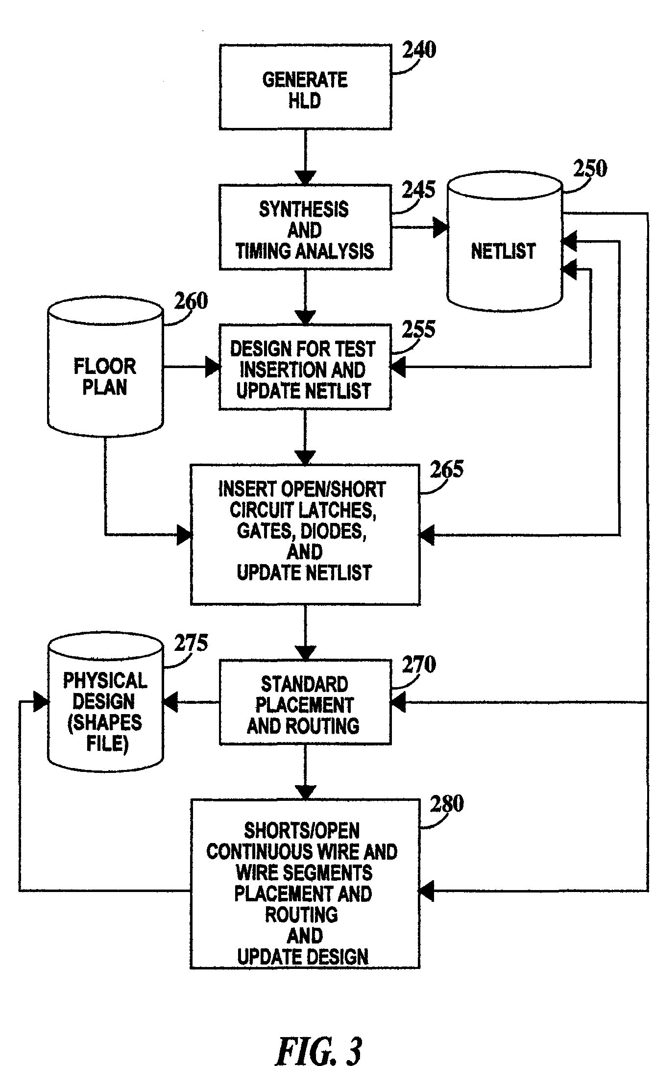
[0022] In the integrated circuit design methodology, circuit elements, including pins are inserted and placed into integrated circuit designs. Insertion is defined as adding the circuit element into the list of elements making up the circuit design and placement is defined as locating the circuit elements relative to the integrated circuit layout or floor plan. Depending upon the software and operating mode used, insertion and placement may be two different operations which may be performed together or at different times or a single operation. Whenever the term placement of an element is used it should be understood that insertion of that element has also occurred.

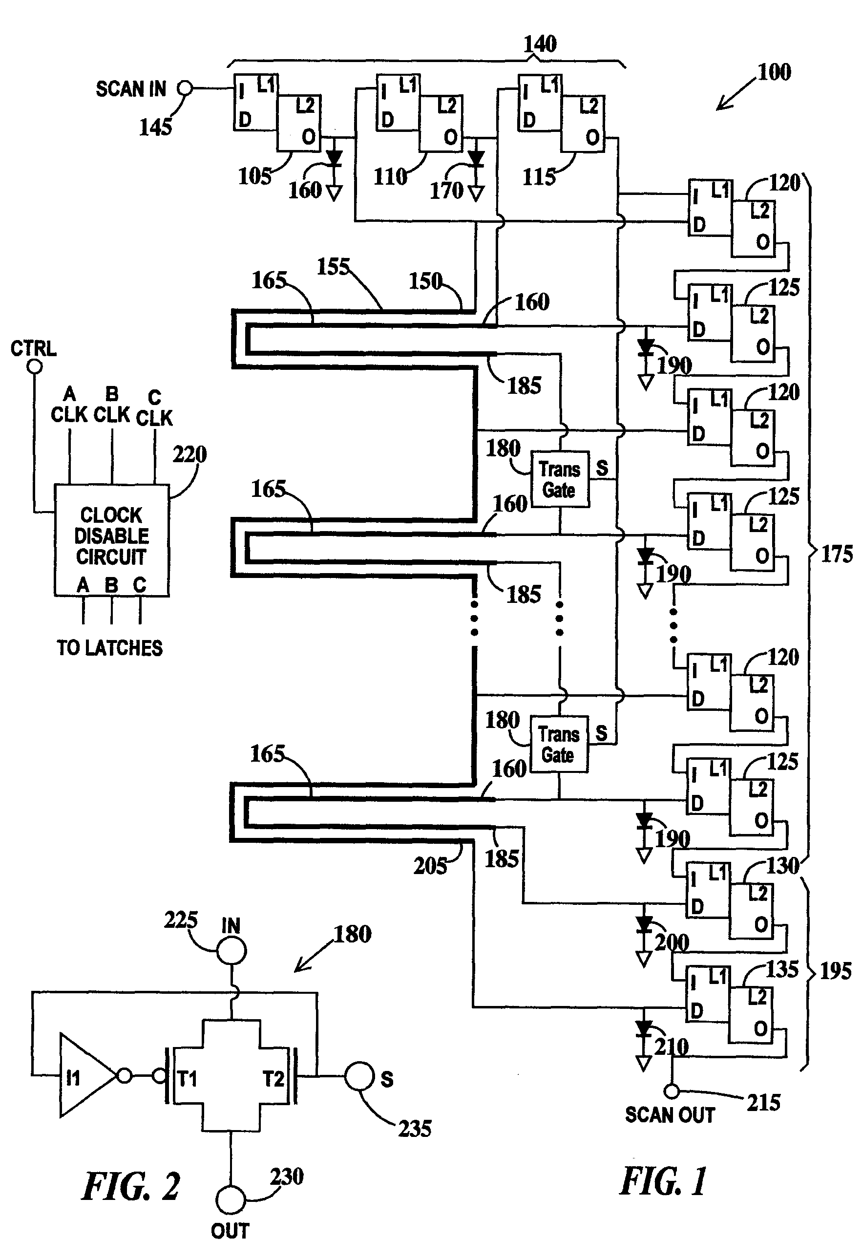
[0023]FIG. 1 is an exemplary circuit and structure for monitoring defects that may be inserted in a an integrated circuit design using the method of the present invention. The circuit illustrated in FIG. 1 monitors defects that can cause opens or shorts between conductive power and / or signal wires of an integrated circuit...


PUM


Abstract

A method and system for designing a test structure. The method including: defining and placing test circuit pins in an integrated circuit design; routing one or more fat wires, each fat wire routed between a set of the test circuit pins; processing each fat wire into a continuous wire and one or more corresponding wire segments adjacent to the continuous wire, the continuous wire separated from the one or more corresponding wire segments by a space; and connecting the continuous wire and the one or more wire segments to circuit elements of a defect monitor scan chain, the circuit elements previously inserted into the integrated circuit design.

Description

CROSS REFERENCE TO RELATED APPLICATIONS [0001] This Application is related to U.S. patent application Ser. No. 10 / 873,012 entitled “Circuit And Method For Monitoring Defects” filed on Jun. 21, 2004, which is hereby incorporated by reference in its entirety.BACKGROUND OF INVENTION [0002] 1. Field of the Invention [0003] The present invention relates to the field of defect monitoring; more specifically, it relates to a method of inserting a test circuit and corresponding shorts / opens defect monitoring structures into an integrated circuit design. [0004] 2. Background of the Invention [0005] Yield management in integrated circuit manufacturing is an ongoing concern and is especially important as new technologies, tools and processes are developed and introduced into manufacturing. As integrated circuits have become more complex, yield learning has become more difficult and defect monitor circuits and structures have become increasing more difficult to insert into integrated circuit chi...

Claims


Application Information

Patent Timeline
IPC IPC(8): G06F17/50G01R31/28
CPCG06F17/505G06F30/327
Inventor COHN, JOHN M.PASTEL, LEAH M.P.
Owner IBM CORP
Why Eureka
Try Eureka