
Source driver, electro-optic device, and driving method

a technology of source driver and electrooptic device, applied in the direction of instruments, static indicating devices, etc., can solve the problems of power consumption, multi-colored images or movies are difficult to be displayed low power consumption is difficult to achieve on the other hand, so as to reduce the cost and reduce the examination cost

Inactive Publication Date: 2006-02-23
SEIKO EPSON CORP
View PDF10 Cites 20 Cited by
  • Summary
  • Abstract
  • Description
  • Claims
  • Application Information

AI Technical Summary

Benefits of technology

The present invention provides a source driver, electro-optic device, and driving method that can realize cost reduction and reduction of examination cost. The invention includes a source driver with impedance conversion circuits and power save data storing circuits, which can inhibit or limit the operating current of the voltage follower circuit based on the power save data. The power save data can be set to the power save data storing circuits or the display data memory, and the invention also provides a method for generating the power save data and setting the impedance conversion circuits. The invention can offer a more efficient and cost-effective source driver for evaluating its performance.

Problems solved by technology

The simple matrix method has an advantage that low power consumption can more easily be achieved compared to the active matrix method on the one hand, and has a disadvantage that multi-colored images or movies are difficult to be displayed on the other hand.
In contrast, the active matrix method has an advantage that it is suitable for displaying multi-colored images or movies on the one hand, and has a disadvantage that low power consumption is difficult to be achieved on the other hand.
However, if the capacitor for preventing oscillation is provided to the operational amplifier, it becomes difficult to shrink the circuit scale.
In particular, if it is applied to the source driver as an output buffer, the operational amplifier is provided for each of, for example, 720 source lines, thus increasing the chip area and making the cost higher.
Incidentally, when the electrical characteristics or the performance of the source driver including the impedance conversion circuits described above, it is difficult to execute examination by connecting testing loads to all the impedance conversion circuits.
However, in this case, the impedance conversion circuits not targeted for the examination remain without loads, and become easy to oscillate if the phase margins of the voltage follower circuits are small, as described above.
And, if the voltage follower circuits included in the impedance conversion circuits not targeted for the examination oscillate, accurate current consumptions of the targeted impedance conversion circuits can not be evaluated, the targeted impedance conversion circuits having the power supply common to the impedance conversion circuits not targeted for the examination.
Further, even if the outputs can be controlled to be high impedance for each block, the examination efficient in terms of cost and time is difficult because the examination needs to be executed for each block.
Therefore, if the voltage follower circuit according to the invention is adopted, the voltage follower circuit of the impedance conversion circuit not targeted for the examination becomes easier to oscillate, and it is difficult to accurately evaluate the electrical characteristics.

Method used


Image

  • Source driver, electro-optic device, and driving method
  • Source driver, electro-optic device, and driving method
  • Source driver, electro-optic device, and driving method

Examples


Embodiment Construction

[0067] Hereinafter, an embodiment of the invention is described in detail with reference to the accompanying drawings. Note that the embodiment described below does not unreasonably limit the content of the invention as claimed in the claim section. Further, not all of the components of the configuration described below are essential elements of the invention.

1. Electro-Optic Device

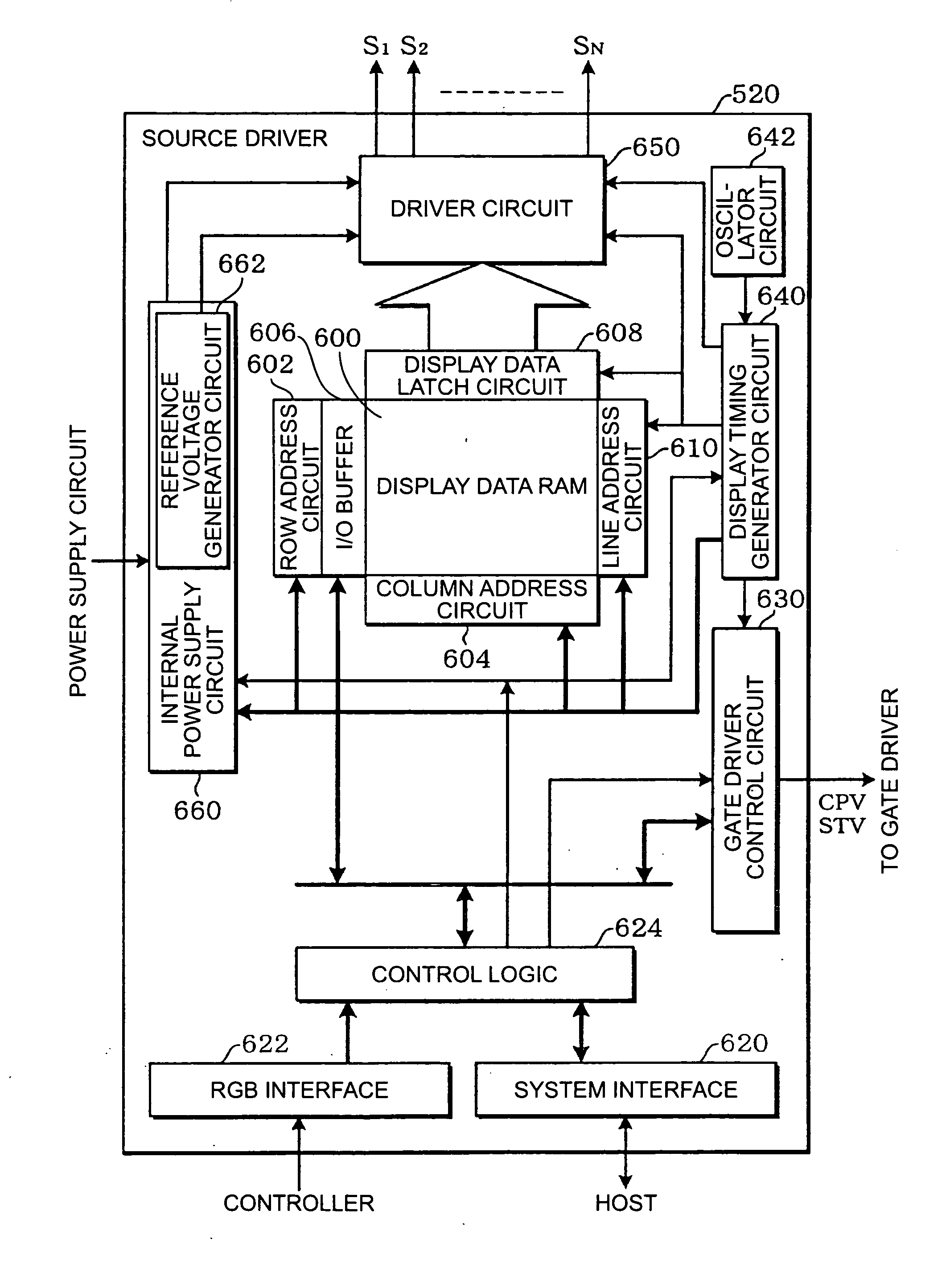
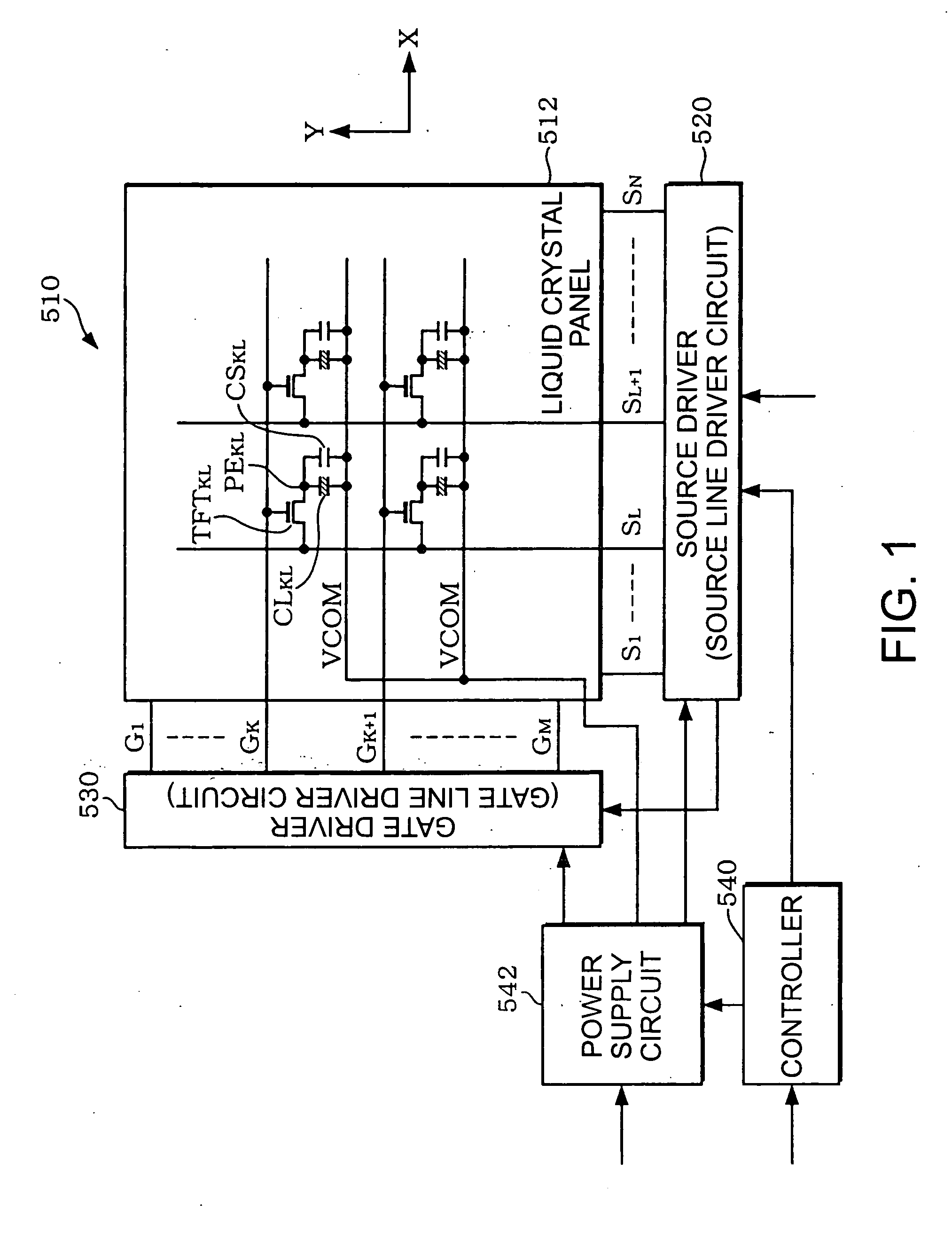
[0068]FIG. 1 shows an example of a block diagram of a display device including an electro-optic device applying the source driver according to the resent embodiment. In FIG. 1, a liquid crystal panel is adopted as the electro-optic device. In FIG. 1, the display device including the liquid crystal panel is defined as a liquid crystal device.

[0069] The liquid crystal device (a display device, in a broad sense) 510 includes a liquid crystal panel (an electro-optic device, in a broad sense) 512, a source driver (a source line driver circuit) 520, a gate driver (a gate line driver circuit) 530, a controll...


PUM


Abstract

A source driver for driving a plurality of source lines of an electro-optic device, including a plurality of impedance conversion circuits each driving a respective one of the plurality of source lines in accordance with a grayscale voltage corresponding to display data; and a plurality of power save data storing circuits each storing power save data, wherein Each of the plurality of power save data storing circuits is provided for one of each of the plurality of impedance conversion circuits and a number of impedance conversion circuits, the number corresponding to the number of dots forming a pixel, each of the plurality of impedance conversion circuits includes a voltage follower circuit for driving one of the plurality of source lines and having a smaller phase margin without a load connected to an output thereof than with a load connected to the output thereof, and, an operating current of the voltage follower circuit included in the impedance conversion circuit is one of stopped and limited in accordance with the power save data stored in the power save data storing circuit corresponding to the impedance conversion circuit.

Description

BACKGROUND OF THE INVENTION [0001] 1. Technical Field [0002] The present invention relates to a source driver, an electro-optic device using the same, and a driving method. [0003] 2. Related Art [0004] In the related art, as liquid crystal panels (electro-optic devices) used for electronic apparatuses such as mobile phones, simple matrix liquid crystal panels and active matrix liquid crystal panels using switching elements such as thin film transistors (hereinafter abbreviated as TFT) are known. [0005] The simple matrix method has an advantage that low power consumption can more easily be achieved compared to the active matrix method on the one hand, and has a disadvantage that multi-colored images or movies are difficult to be displayed on the other hand. In contrast, the active matrix method has an advantage that it is suitable for displaying multi-colored images or movies on the one hand, and has a disadvantage that low power consumption is difficult to be achieved on the other h...

Claims


Application Information

Patent Timeline
Patent Type & Authority Applications(United States)
IPC IPC(8): G09G3/36
CPCG09G2310/027G09G3/3688G09G3/36G09G3/20
Inventor TAKAHASHI, MASAMIMAKI, KATSUHIKO
Owner SEIKO EPSON CORP
Learn More