Driving circuit, driving method of electro-optical device, electro-optical device, and electronic apparatus

a driving circuit and driving method technology, applied in the direction of optics, digital storage, instruments, etc., can solve the problems of delay in the output timing of sampling signals and deterioration of display quality, so as to reduce the number of logical operations and shorten the signal path. , the effect of high quality

Inactive Publication Date: 2006-02-23
SEIKO EPSON CORP
View PDF4 Cites 0 Cited by
  • Summary
  • Abstract
  • Description
  • Claims
  • Application Information

AI Technical Summary

Benefits of technology

[0010] An advantage of the invention is that it provides a driving circuit and a driving method of an electro-optical device, which is capable of performing an image display with high quality, an electro-optical device including the driving circuit, and various electronic apparatus including the electro-optical device.
[0011] According to an aspect of the invention, a driving circuit of the electro-optical device has a plurality of scanning lines, a plurality of data lines, and a plurality of pixel electrodes electrically connected to the scanning lines and the data lines, respectively, in an image display region on a substrate. The driving circuit includes a shift register circuit which sequentially outputs transfer signals from respective stages, a first arithmetic logic circuit which outputs the sequentially output transfer signals and selection signals for precharge input from a first input terminal to a first path by a logical operation, a second arithmetic logic circuit which generates sampling signals by a logical operation between the transfer signals input from the first path and enable signals input from a second input terminal and outputs the generated sampling signals and which the selection signals for precharge input from the first path to a second path, and a sampling circuit including a plurality of sampling switches which sample precharge signals, which are supplied via an image signal line and have precharge potentials, according to the selection signals for precharge supplied via the second path and supplies the sampled signals to the data lines, respectively, and sample image signals, which are supplied via the image signal line and have display potentials, according to the sampling signals supplied via the second path and supplies the sampled signals to the data lines, respectively.
[0012] According to the driving circuit of the electro-optical device of the invention, during the time of driving the electro-optical device, the shift register circuit sequentially generates the transfer signals and outputs them on the basis of the various timing signals supplied from an external circuit.
[0013] In the above-mentioned structure, it is preferable that the first and second arithmetic logic circuit are disposed corresponding to respective stages of the shift register. The first arithmetic logic circuit is supplied with the selection signals for precharge from an external circuit and the transfer signals output from the shift register circuit, via the first input terminal thereof. The first arithmetic logic circuit outputs the input transfer signals and the selection signals for precharge to the first path through the logical operation.
[0014] Further, the second arithmetic logic circuit is supplied with the enable signals from an external circuit via the second input terminal, and the transfer signals and the selection signals for precharge from the first path, via the first input terminal. The second arithmetic logic circuit generates the sampling signals through the logical operation between the transfer signals and the enable signals supplied thereto. The selection signals for precharge and the sampling signals are output to the second path from the second arithmetic logic circuit.
[0015] Therefore, according to the driving circuit of the invention, it is possible to reduce the number of logical operations using the enable signals input to the second input terminal, compared to the number of logical operations until the selection signals for precharge are output to the second path after they are input the first input terminal. Further, it is possible to shorten the signal path until the sampling signals are output to the second path after the enable signals are input the second input terminal, compared to the signal path until the selection signals for precharge are output to the second path after they are input to the first input terminal.

Problems solved by technology

However, in case of performing the above-described precharge, an output timing of the sampling signal may be delayed with respect to an input timing of the enable signal in each arithmetic logic circuit.
In this way, when the output timing of the sampling signal is delayed in the arithmetic logic circuit, ON and OFF of the sampling switch is delayed, such that a display irregularity is generated in addition to that the ghosting is viewed on display, thereby deteriorating the display quality.

Method used


Image

  • Driving circuit, driving method of electro-optical device, electro-optical device, and electronic apparatus
  • Driving circuit, driving method of electro-optical device, electro-optical device, and electronic apparatus
  • Driving circuit, driving method of electro-optical device, electro-optical device, and electronic apparatus

Examples


Embodiment Construction

[0054] The operation and another advantage of the invention will be apparent from embodiments to be described below.

[0055] Hereinafter, preferred embodiments of the invention will be described with reference to the accompanying drawings. In the embodiments to be described, the electro-optical device of the invention is applied to a liquid crystal device.

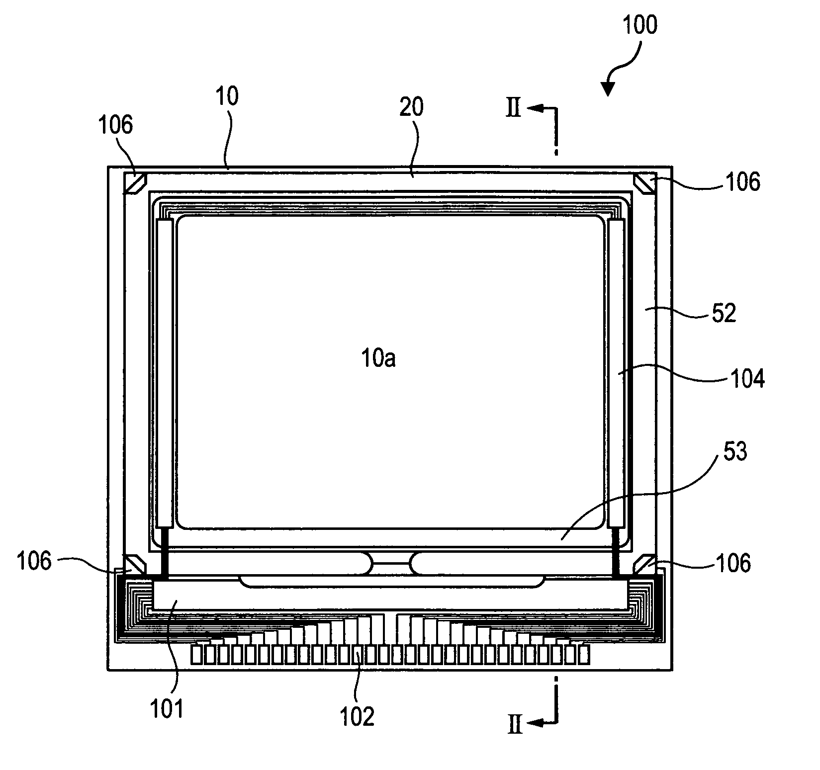
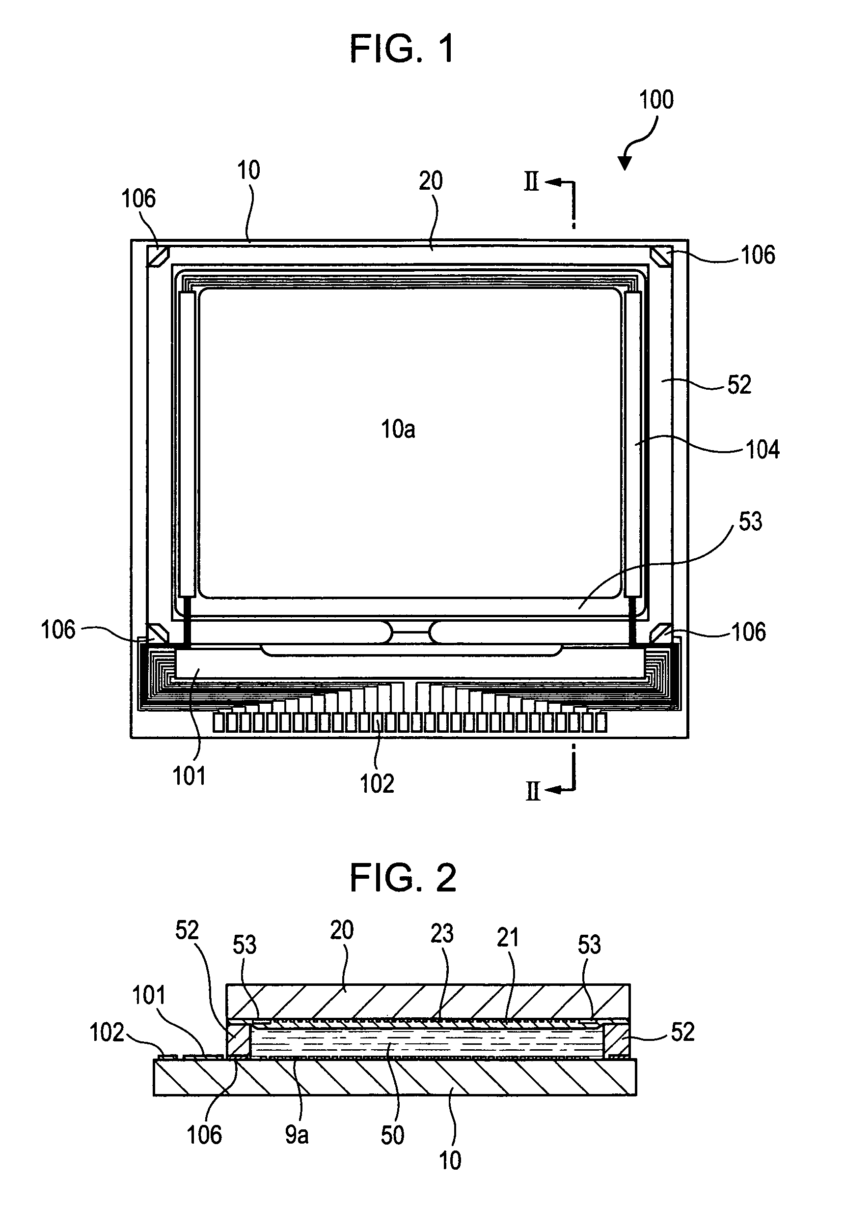
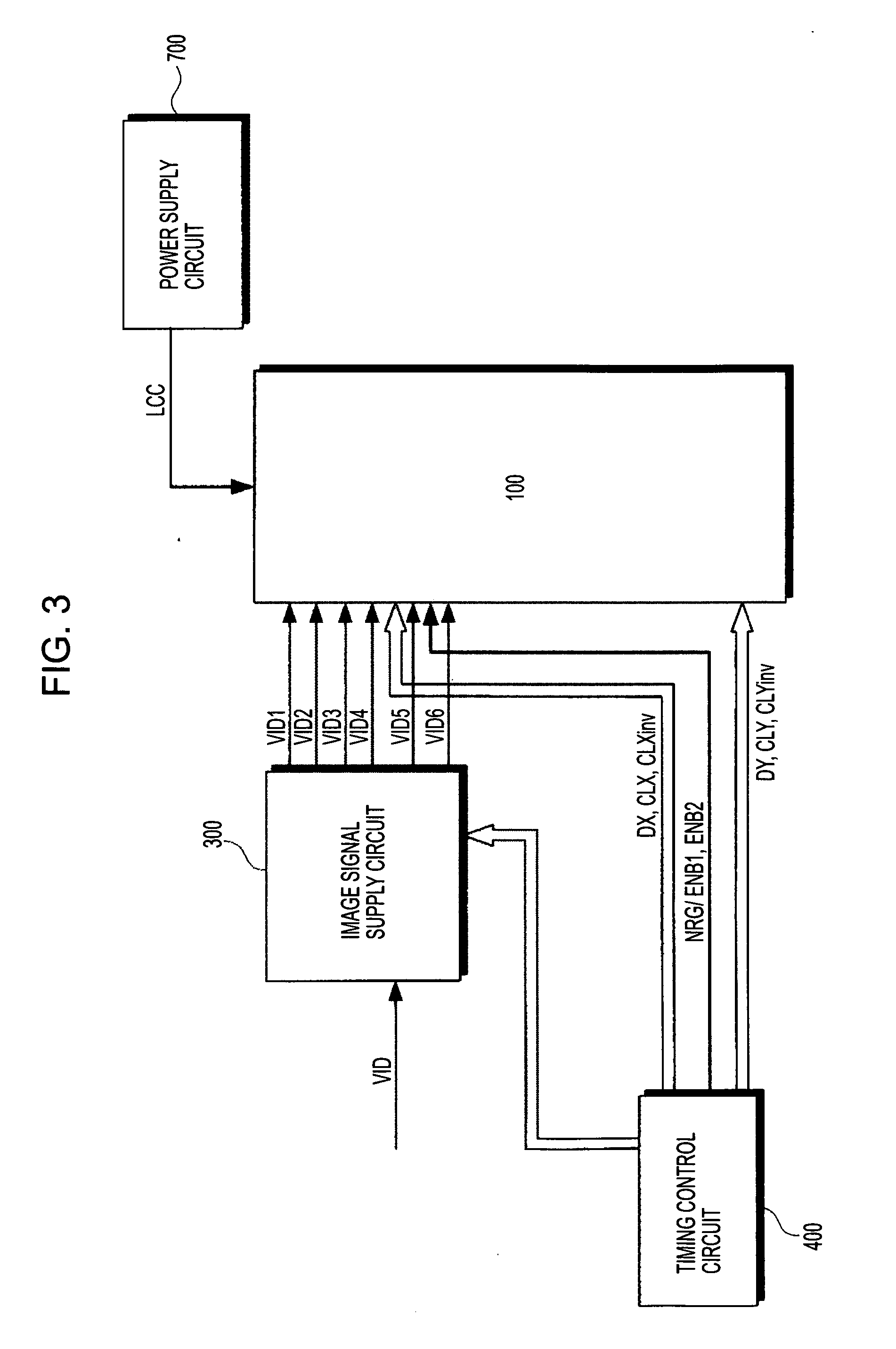
[0056] First, in a liquid crystal device which is an example of the invention, the entire construction of a liquid crystal panel as an example of an electro-optical panel will be described with reference to FIGS. 1 and 2. Here, FIG. 1 is a schematic plan view of the liquid crystal panel, in which a TFT array substrate is seen from a counter substrate together with each element formed on a TFT array substrate, and FIG. 2 is a cross-sectional view taken along the line II-II of FIG. 1. Here, a TFT active matrix driving type liquid crystal device with built-in driving circuits will be described as an example.

[0057] In FIGS. 1 and 2, t...


PUM


Abstract

A driving circuit of an electro-optical device having a plurality of scanning lines, a plurality of data lines, and a plurality of pixel electrodes electrically connected to the scanning lines and the data lines, respectively, in an image display region on a substrate, the driving circuit includes a shift register circuit which sequentially outputs transfer signals from respective stages, a first arithmetic logic circuit which outputs the sequentially output transfer signals and selection signals for precharge input from a first input terminal to a first path by a logical operation, a second arithmetic logic circuit which generates sampling signals by a logical operation between the transfer signals input from the first path and enable signals input from a second input terminal, and which outputs the generated sampling signals and the selection signals for precharge input from the first path to a second path, and a sampling circuit including a plurality of sampling switches which sample precharge signals, which are supplied via an image signal line and have precharge potentials, according to the selection signals for precharge supplied via the second path, and supplies the sampled signals to the data lines, respectively, and sample image signals, which are supplied via the image signal line and have display potentials, according to the sampling signals supplied via the second path, and which supplies the sampled signals to the data lines, respectively.

Description

BACKGROUND OF THE INVENTION [0001] 1. Technical Field [0002] The invention relates to a driving circuit and to a driving method for driving an electro-optical device such as a liquid crystal device, to an electro-optical device including the driving circuit, and to an electronic apparatus such as a liquid crystal projector which has the electro-optical device provided therein. [0003] 2. Related Art [0004] The electro-optical device driven by the driving circuit includes a plurality of data lines, a plurality of scanning lines, and pixel electrodes which are electrically connected to the data lines and the scanning lines, respectively, and are provided to every pixel portion, in an image display region on a substrate. [0005] According to Japanese Unexamined Patent Application Publication Nos. 10-282938, 2001-356746, 2002-297105, 2002-297106, and 11-65536, during the time of driving the electro-optical device, a sampling signal is generated in the driving circuit by performing a wavef...

Claims


Application Information

Patent Timeline
Patent Type & Authority Applications(United States)
IPC IPC(8): G11C7/00
CPCG09G3/3688G09G2320/0257G09G2310/0297G09G2310/0248G09G3/36G02F1/13G09G3/20
Inventor YAMASAKI, YASUJI
Owner SEIKO EPSON CORP
Why Eureka
Try Eureka