Light-emitting device and production method thereof

a technology of light-emitting devices and production methods, which is applied in the direction of identification means, instruments, discharge tubes, etc., can solve the problems of reliability and durability, difficult formation of glass substrates and plastic substrates, and limited application range, and achieve excellent light-emitting efficiency, stability and production cost.

Inactive Publication Date: 2006-03-02
CANON KK
View PDF11 Cites 24 Cited by
  • Summary
  • Abstract
  • Description
  • Claims
  • Application Information

AI Technical Summary

Benefits of technology

[0013] It is, therefore, an object of the present invention to provide a novel light-emitting device which is excellent in light emission efficiency, stability and production cost.

Problems solved by technology

A light-emitting diode can be driven with a low voltage and is excellent in stability, but requires high temperature process for crystal growth, and is therefore difficult to be formed on a glass substrate and a plastic substrate.
Therefore, as a display, its range of application is limited.
An organic EL display can be driven with a low voltage and can be formed on a glass substrate or a plastic substrate, but has a problem in reliability and durability.
With regard to inorganic display, production of a large area display is comparatively easy, and high resistance to use environment can be expected, but the high drive voltage is currently problematic.

Method used


Image

  • Light-emitting device and production method thereof
  • Light-emitting device and production method thereof
  • Light-emitting device and production method thereof

Examples


example 1

[0097] A light-emitting device of the present example has a configuration similar to the configuration shown in FIGS. 1A and 1B.

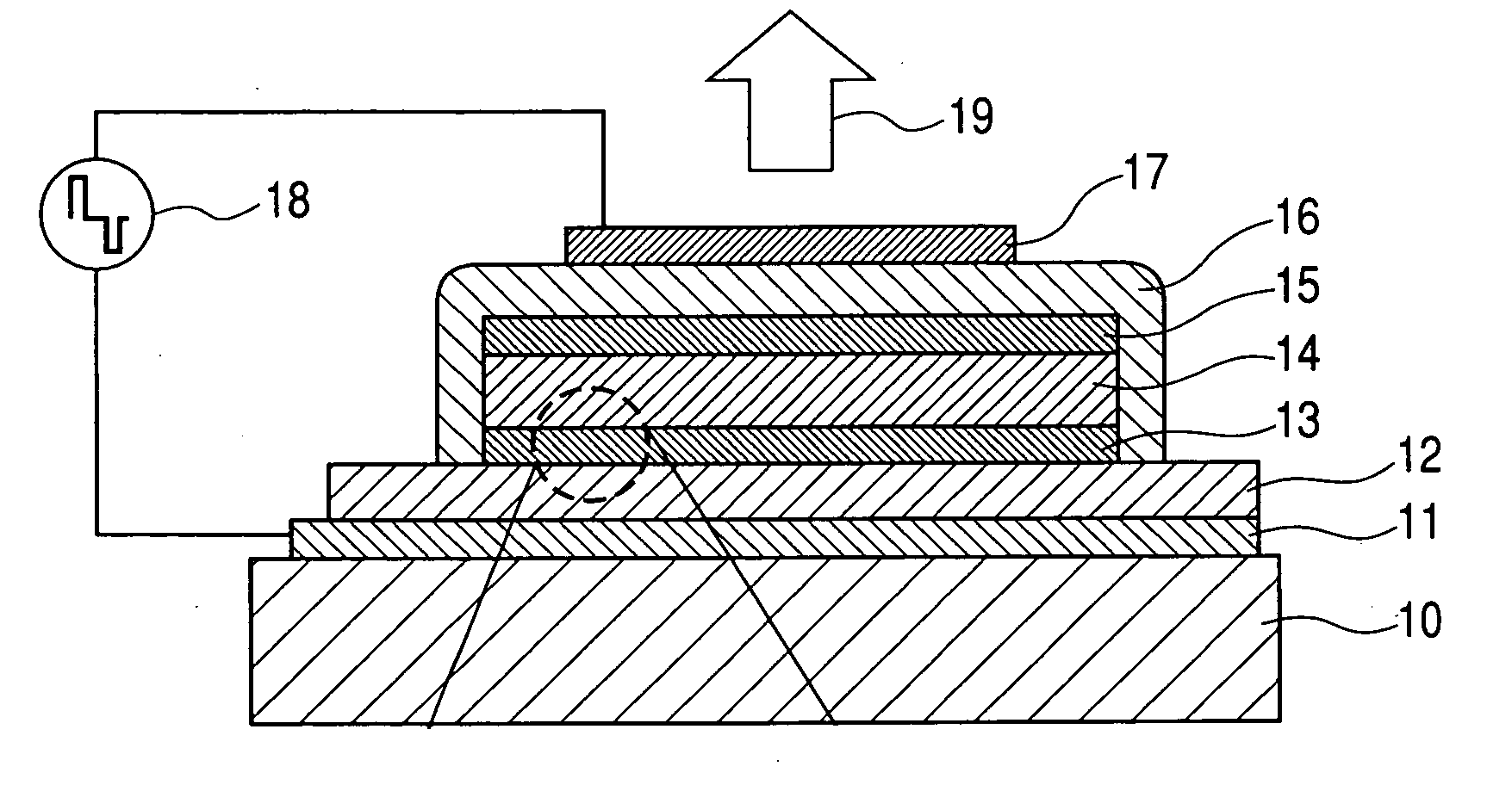
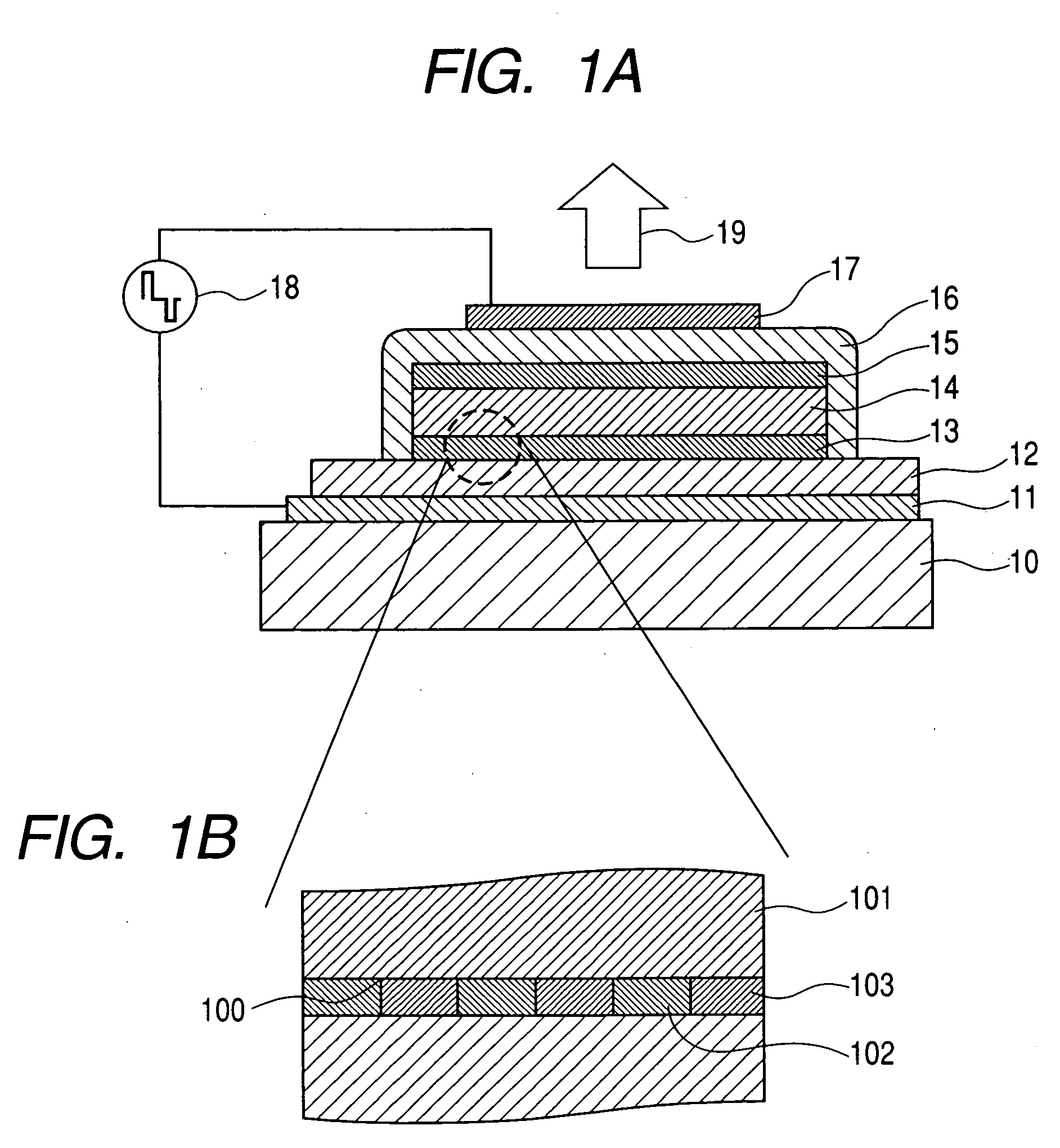
[0098]FIG. 1A is a schematic view showing a configuration of a light-emitting device in accordance with the present invention, and FIG. 1B is an enlarged view of a portion indicated by a chain circle in FIG. 1A.

[0099] In the figures, reference numeral 10 denotes a substrate; reference numeral 11 denotes an electrode layer; reference numeral 12 denotes a first insulating layer; reference numeral 13 denotes a first fine-structured layer; reference numeral 14 denotes a light emitting layer; reference numeral 15 denotes a second fine-structured layer; reference numeral 16 denotes a second insulating layer; reference numeral 17 denotes a transparent electrode layer (second-electrode layer); reference numeral 18 denotes a power supply; and reference numeral 19 denotes light. However, the present example is configured with the first insulating layer 12 and the s...

example 2

[0113] A light-emitting device of the present example has a configuration similar to the configuration shown in FIGS. 1A and 1B.

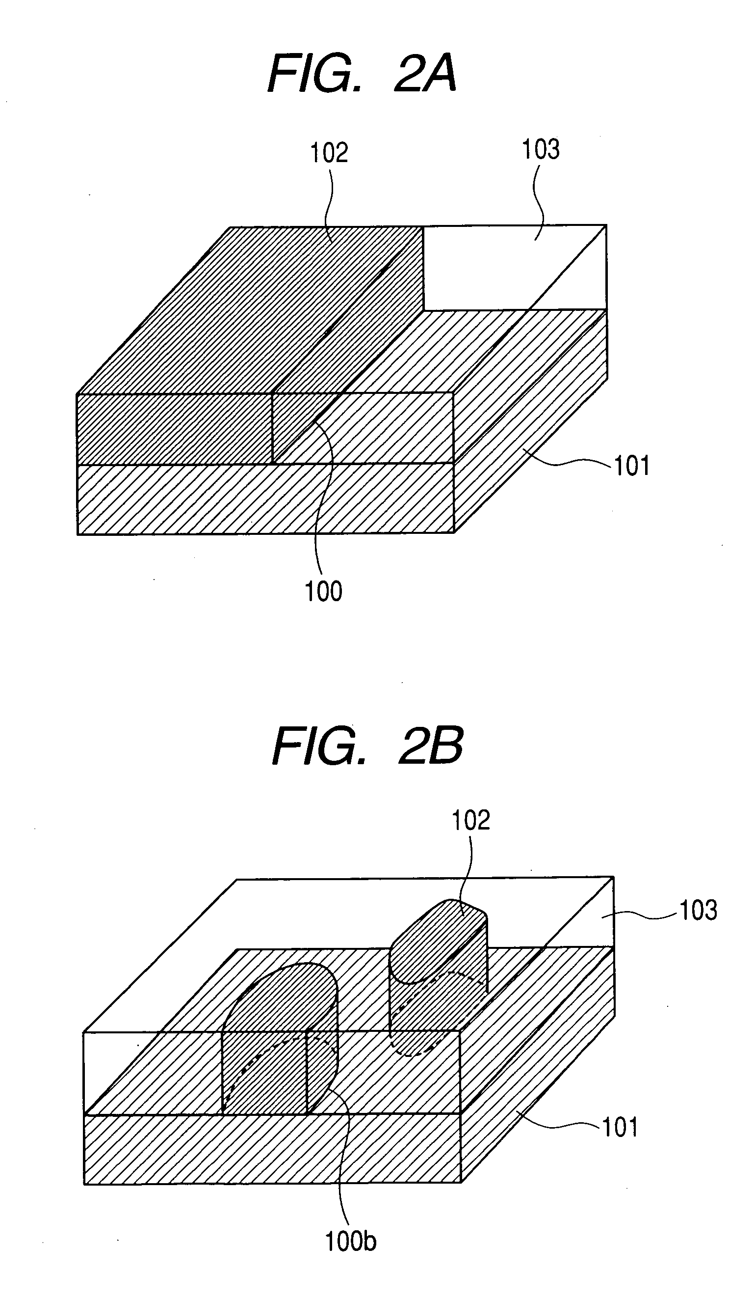
[0114] As shown in FIG. 7B, the fine-structured layer of the present example has, inside the layer plane, a first part 21 consisting of a first material and a second part 22 consisting of a second material. The first part 21 and the second part 22 in FIG. 7B respectively correspond to the second part 102 and the third part 103 in FIGS. 1A and 1B. Further, the first material contains iron oxide (dielectric constant: about 12 to 16) as a main component, while the second material contains silicon oxide (dielectric constant: ˜4) as a main component. A number of triple junctions with geometry of a closed line will be disposed at an interface between the fine-structured layer and the light-emitting layer (the first part of the first dielectric constant). Incidentally, the light-emitting layer is made of Y2O3:Eu (dielectric constant: ˜12)

[0115] In this example, ...

example 3

[0125] A light-emitting device of the present example has a configuration similar to the configuration shown in FIGS. 1A and 1B.

[0126] However, the present example is configured with the first insulating layer 12 and the second insulating layer 16 being omitted, since the fine-structured layers have a sufficient insulating property.

[0127] In addition, the electrode layer 11 is formed of a transparent electrode, and the present example is a light-emitting device of a type in which a light is taken out from the rear side of the substrate.

[0128] As shown in FIG. 7C, the fine-structured layer of the present example has, inside the layer plane, a first part 21 consisting of a first material and.:a second part 22 consisting of a second material. The first part 21 and the second part 22 in FIG. 7C respectively correspond to the second part 102 and the third part 103 in FIGS. 1A and 1B. Further, the first material contains zirconia (dielectric constant: about 20 to 25) as a main componen...


PUM


Abstract

A light-emitting device is provided that is excellent in light emission efficiency and stability. The light-emitting device has a first part of a first dielectric constant, a second part of a second dielectric constant and a third part of a third dielectric constant, and has a triple junction where they are in contact with one another. Moreover, a first and a second electrode are provided for applying a voltage for controlling an electric field at the triple junction and in the vicinity thereof. Further, at least one of the first, the second and the third parts is a constituted by light-emitting material, and the triple junction forms a closed line.

Description

BACKGROUND OF THE INVENTION [0001] 1. Field of the Invention [0002] The present invention relates to a light-emitting device and a production method thereof. [0003] 2. Related Background Art [0004] As a light-emitting device, two types of devices are known. [0005] One is a device of current injection type, in which carrier (electron and holes) are injected into p-n junction and light is emitted by electron-hole recombination. This type of devices of a light emitting diode and a laser diode etc. is operated under relatively low voltages (<10V) and may be driven under DC condition. [0006] Another is a device using electric field excitation, in which high electric field across stacked dielectric layer and light-emitting layer is used to accelerate electrons and excite the light-emitting layer. This type of device of inorganic EL etc. is operated under relatively high voltages and is driven under AC condition. A general inorganic EL has a double insulating structure with an electrode...

Claims


Application Information

Patent Timeline
Patent Type & Authority Applications(United States)
IPC IPC(8): H01L33/00H01J1/62G09F9/30H01L27/32H05B33/10H05B33/14H05B33/22
CPCC09K11/574H05B33/22H01L2251/564H01L51/52H10K50/80H10K71/841
Inventor IWASAKI, TATSUYADEN, TOHRUOIKAWA, KATSUYA
Owner CANON KK
Why Eureka
Try Eureka