Voltage translator with data buffer

a voltage translator and buffer technology, applied in logic circuits, logic circuit coupling/interface arrangements, pulse techniques, etc., can solve problems such as the difficulty of tuning the voltage translator, the influence of several factors, and the reliability and delay of wide voltage ranges,

Inactive Publication Date: 2006-03-02
IBM CORP
View PDF5 Cites 11 Cited by
  • Summary
  • Abstract
  • Description
  • Claims
  • Application Information

AI Technical Summary

Benefits of technology

[0010] A principal aspect of the present invention is to provide a voltage translator with a data buffer. Other important aspects of the present invention are to provide such voltage translator with a data buffer substantially without negative effect and that overcome some of the disadvantages of prior art arrangements.

Problems solved by technology

A problem with many voltage translators is reliability and delay over wide voltage ranges, temperature ranges, and process lots.
A problem with the conventional voltage translator of FIG. 1 is the difficulty to tune the voltage translator.
Modifying one transistor of the conventional voltage translator of FIG. 1 typically has too great an affect on several factors that might not need to be changed.
However, then the switch point of the output inverter is lower so that the output falling delay is faster while the rising delay slows down.
Further for example, if the width of NFET 106 is increased to improve the rising delay, this also decreases the output falling delay and slows down the output falling slew rate.
Another problem with the conventional voltage translator of FIG. 1 is the difficulty to switch states of the cross-coupled inverter circuit.

Method used


Image

  • Voltage translator with data buffer
  • Voltage translator with data buffer
  • Voltage translator with data buffer

Examples


Embodiment Construction

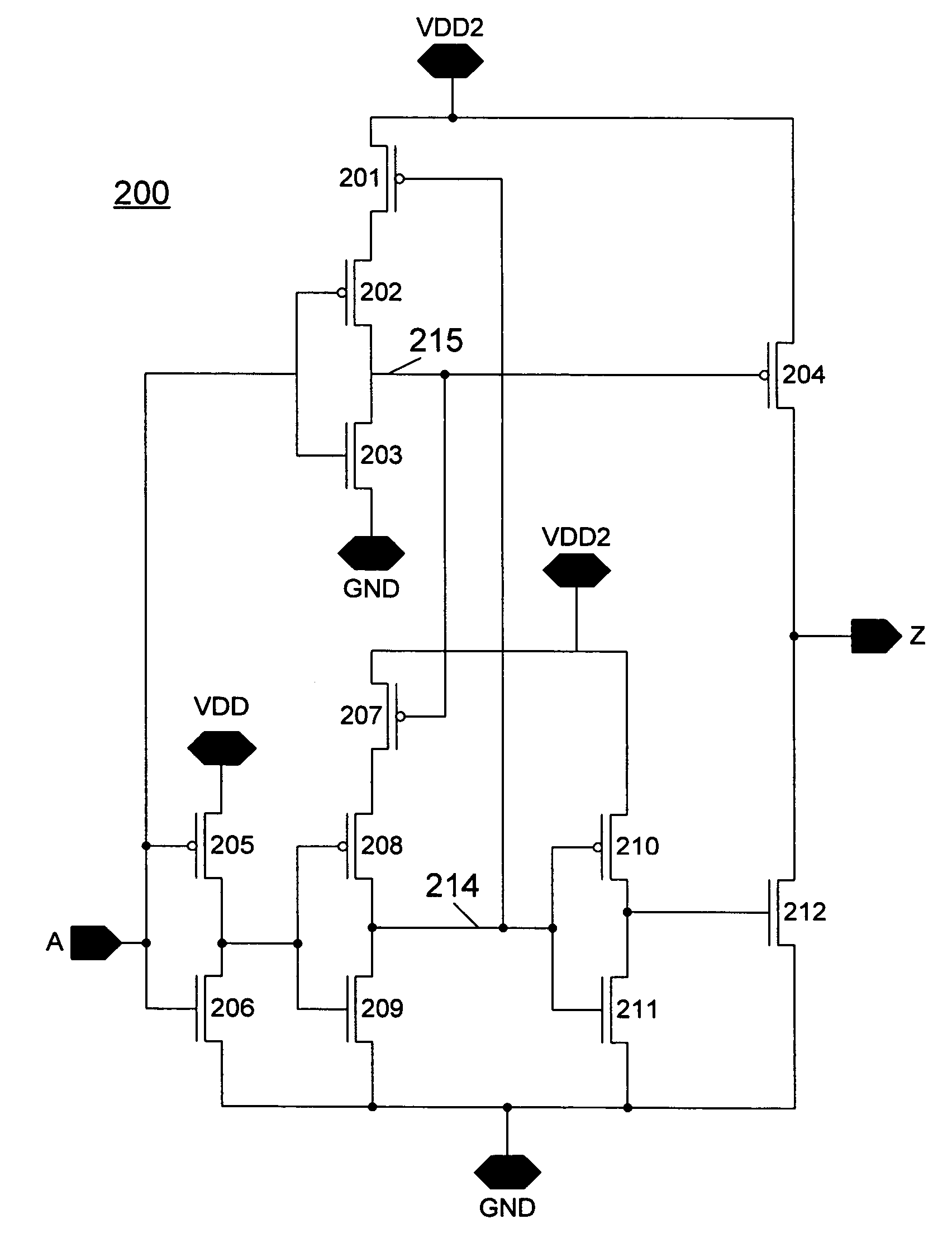
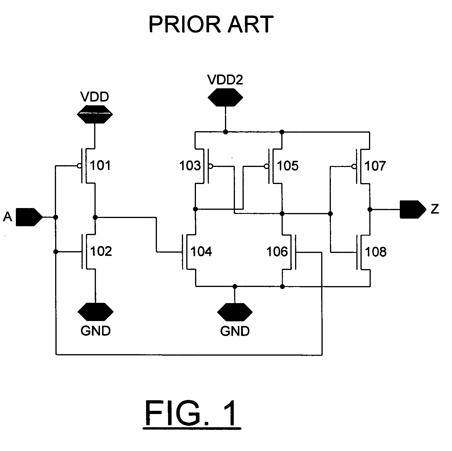
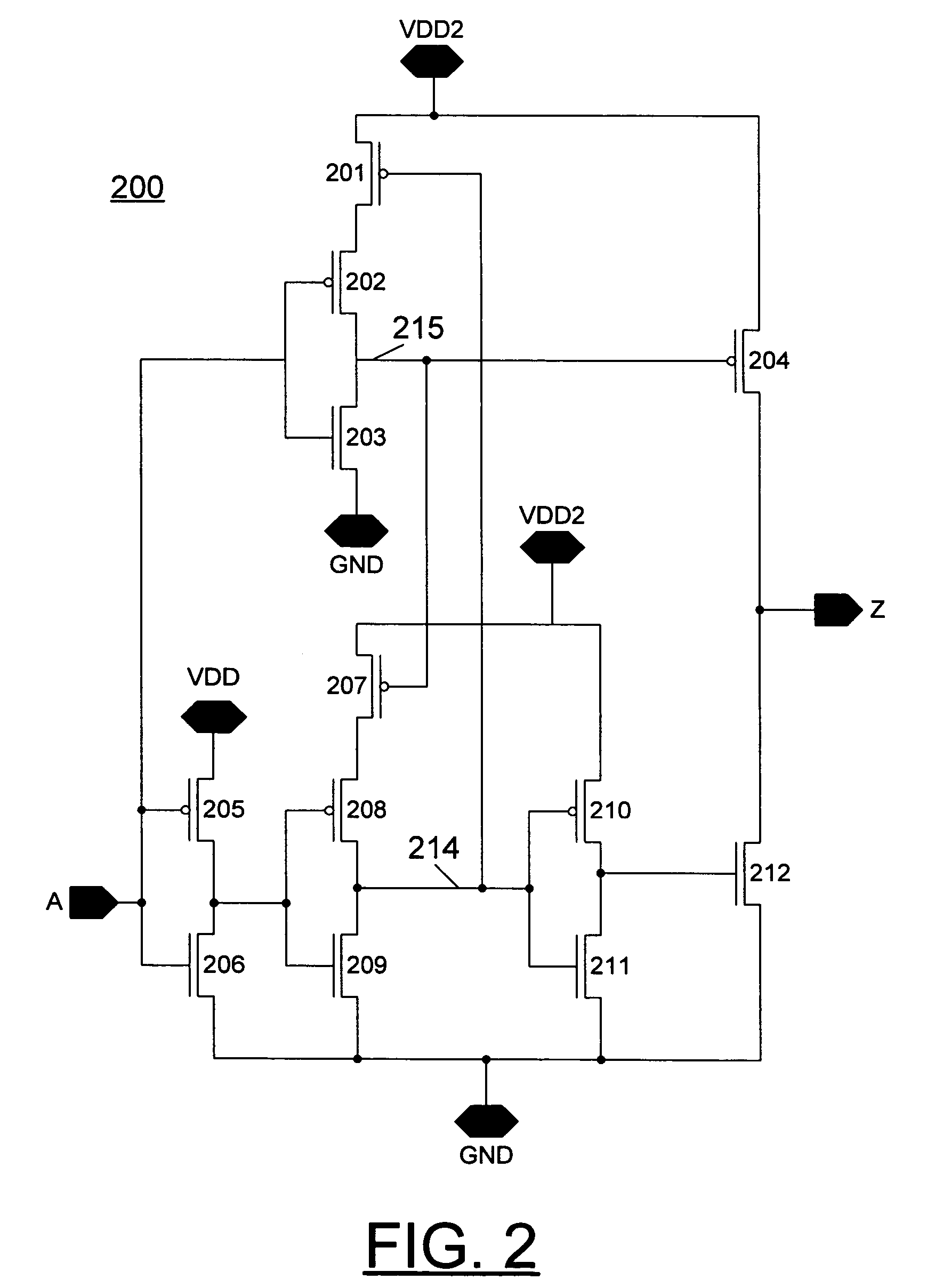
[0017] In accordance with features of the preferred embodiment a voltage translator, as illustrated and described with respect to FIG. 2, provides improved tuning enabling balanced operation of an output stage as compared to the prior art voltage translator of FIG. 1. The voltage translator in accordance with the preferred embodiment includes a cross-coupled NOR topology instead of the cross-coupled inverter circuit of the prior art voltage translator of FIG. 1. The cross-coupled NOR topology of the preferred embodiment enables significantly faster switching as compared to the cross-coupled inverter circuit of the prior art voltage translator of FIG. 1. An output PFET and an output NFET of the voltage translator of the preferred embodiment are driven separately, providing enhanced flexibility for tuning both delay and slew rate. Also since an output PFET and an output NFET of the voltage translator of the preferred embodiment are driven separately, shoot through current can be elimi...


PUM


Abstract

A voltage translator with data buffer includes an input inverter receiving a data input signal at a first voltage level. A level shifting cross-coupled NOR circuit is coupled to the input inverter for translating the data input signal at a second voltage level. An output stage driven by the level shifting cross-coupled NOR circuit for providing a data output signal at the second voltage level. The voltage translator enables improved performance across various power, voltage and temperature (PVT) conditions and reliably reduces or minimizes shoot through current and delay.

Description

FIELD OF THE INVENTION [0001] The present invention relates generally to the integrated circuit design field, and more particularly, relates to a voltage translator with data buffer. DESCRIPTION OF THE RELATED ART [0002] Various voltage translator or voltage level shifter arrangements are known. A voltage translator translates data from one voltage to another voltage, typically from a lower to higher voltage. The voltage translator also is useable as an output buffer adapted for minimizing shoot through current. [0003] Voltage translators are widely used. Many voltage translators use latching mechanisms to eliminate DC current after the data has been translated. [0004] A problem with many voltage translators is reliability and delay over wide voltage ranges, temperature ranges, and process lots. [0005]FIG. 1 illustrates a conventional voltage translator. The conventional voltage translator includes an input A applied to a gate input of an input inverter defined by a series connected...

Claims


Application Information

Patent Timeline
Patent Type & Authority Applications(United States)
IPC IPC(8): H03K19/0175
CPCH03K3/356104H03K3/356113H03K19/018521H03K17/08122H03K19/00384H03K3/356165
Inventor CHEN, DAVID JIAKERR, MICHAEL KEVINLAWSON, WILLIAM FREDERICK
Owner IBM CORP
Why Eureka
Try Eureka